
Semiconductor plasma etching technology

A plasma and process technology, which is applied in the field of semiconductor manufacturing process, can solve the problems of affecting the etching result, unfavorable, affecting the relative position relationship of graphics, etc., to achieve the effect of reducing lateral etching, increasing the selection ratio, and avoiding over-etching

Active Publication Date: 2009-12-30
BEIJING NAURA MICROELECTRONICS EQUIP CO LTD
View PDF0 Cites 8 Cited by
  • Summary
  • Abstract
  • Description
  • Claims
  • Application Information

AI Technical Summary

Problems solved by technology

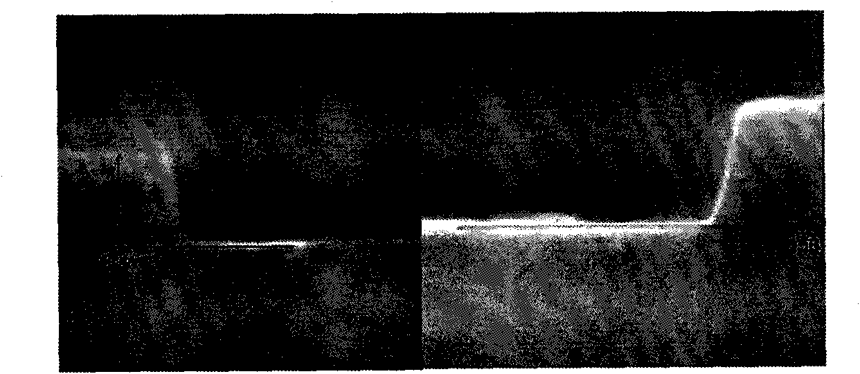
Because the photoresist has a wide coverage, there are more carbon-containing by-products in the etching process, which is not conducive to etching a section with a steep angle, and a thin hard mask layer is not conducive to protecting the top of the silicon line, so that the edge of the line is prone to rounding. Angle, which makes it difficult to achieve the desired result of etching
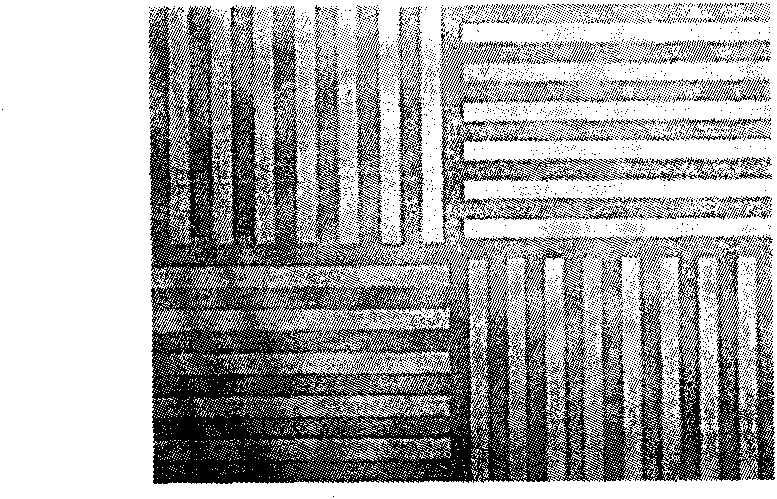
[0007] Further, when the aforementioned etching result pattern is used as a zero mark for interlayer etching calibration, if its section is not steep enough and has edge fillets, it will not only affect the etching result this time, but will further Affects the effect of photolithography calibration, that is, affects the relative positional relationship of patterns between layers

Method used


Image

  • Semiconductor plasma etching technology
  • Semiconductor plasma etching technology
  • Semiconductor plasma etching technology

Examples


Embodiment Construction

[0033] In order to make the above objects, features and advantages of the present invention more comprehensible, the present invention will be further described in detail below in conjunction with the accompanying drawings and specific embodiments.

[0034] refer to Figure 4 , shows a specific example of a plasma etching process of the present invention, which may include the following two-step etching process:

[0035] The dielectric layer runs through the etching step 401, and the process gas used for the dielectric layer passing through the etching step includes a fluorine-based etching gas, a first photoresist protection gas, and a dilution gas;

[0036] Silicon main etching step 402 , the process gas in the silicon main etching step includes main etching gas, carbon-based by-product removal gas and second photoresist protection gas.

[0037] Since usually the wafer is also covered with a hard dielectric layer on the substrate silicon layer, for example, the usual hard d...


PUM


Abstract

The invention provides a plasma etching technology comprising a dielectric layer penetrating and etching step and a silicon main etching step, wherein, technical gas in the dielectric layer penetrating and etching step comprises fluorine-base etching gas, first light resistance protection gas and dilution gas; technical gas in the silicon main etching step comprises main etching gas, carbon-base by-product removing gas and second light resistance protection gas. In a preferable embodiment, the fluorine-base etching gas is CF4 or SF6, the first light resistance protection gas is CH2F2 or CHF3 or HBr, and the dilution gas is He, Ar or N2; the main etching gas is Cl2, the carbon-base by-product removing gas is O2, and the second light resistance protection gas is HBr. In semiconductor plasma etching, the invention can improve sidewall steepness in figure etching and prevent the upper edge and the lower edge of a line from producing fillets.

Description

technical field [0001] The invention relates to the technical field of semiconductor manufacturing technology, in particular to an improved semiconductor plasma etching technology. Background technique [0002] Plasma etching (also known as dry etching) is one of the key processes in integrated circuit manufacturing, and its purpose is to completely copy the mask pattern to the surface of the silicon wafer (wafer). [0003] The principle of plasma etching can be summarized as the following steps: (1) Under low pressure, the reaction gas is excited by radio frequency power to generate ionization and form plasma (plasma is composed of charged electrons and ions), and the reaction chamber Under the impact of electrons, the gas in the body can not only transform into ions, but also absorb energy and form a large number of active groups (Radicals); (2) The active reactive groups form a chemical reaction with the surface of the etched material and form volatile (3) The reaction p...

Claims


Application Information

Patent Timeline
Patent Type & Authority Applications(China)
IPC IPC(8): H01L21/311H01L21/3065
Inventor 李俊杰杨盟
Owner BEIJING NAURA MICROELECTRONICS EQUIP CO LTD
Learn More