Semiconductor device and manufacturing method thereof, integrated circuit and electronic device

A manufacturing method and semiconductor technology, applied in semiconductor/solid-state device manufacturing, semiconductor devices, circuits, etc., can solve the problems of increasing the production cost of gate-all-around devices, complex processes, and high manufacturing difficulty

Pending Publication Date: 2020-10-20
INST OF MICROELECTRONICS CHINESE ACAD OF SCI
View PDF0 Cites 5 Cited by
  • Summary
  • Abstract
  • Description
  • Claims
  • Application Information

AI Technical Summary

Problems solved by technology

However, the internal wall technology has complicated procedures and high manufacturing difficulty, which will also increase the production cost of gate-all-around devices.

Method used


Image

  • Semiconductor device and manufacturing method thereof, integrated circuit and electronic device
  • Semiconductor device and manufacturing method thereof, integrated circuit and electronic device
  • Semiconductor device and manufacturing method thereof, integrated circuit and electronic device

Examples


Embodiment Construction

[0088] The specific implementation manners according to the present invention will be described below in conjunction with the accompanying drawings. In the following description, many specific details are set forth in order to fully understand the present invention, but the present invention can also be implemented in other ways different from those described here, therefore, the present invention is not limited to the specific embodiments disclosed below limit.

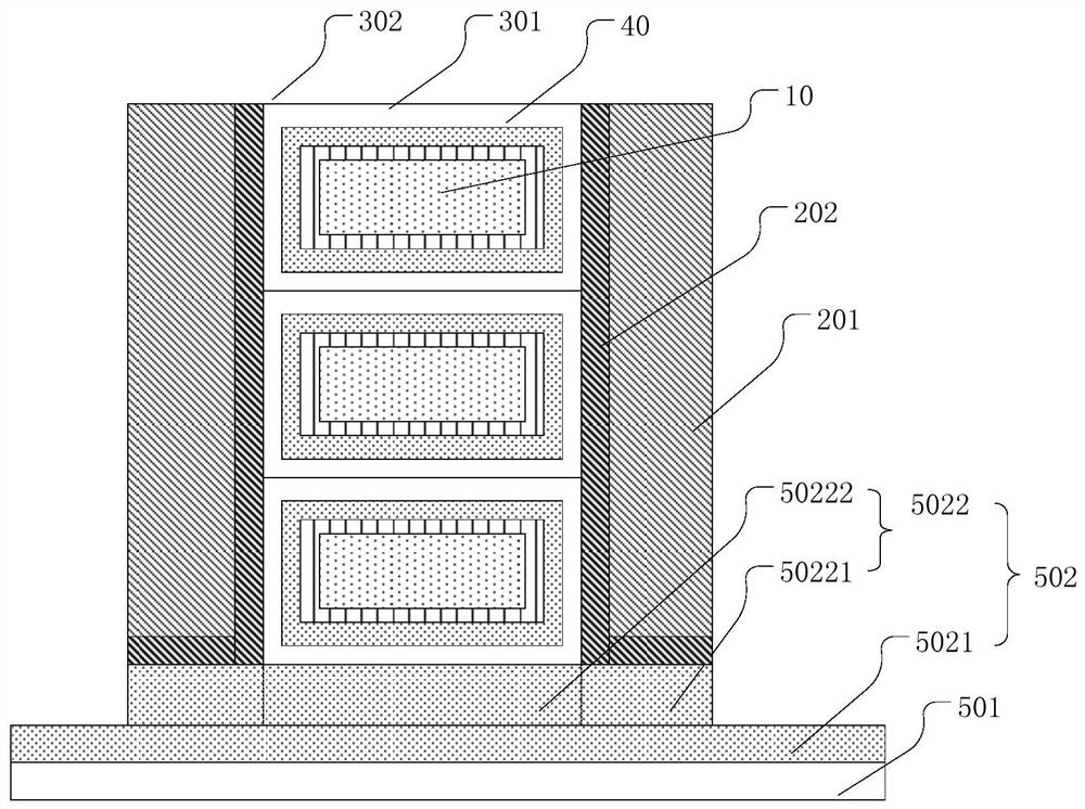
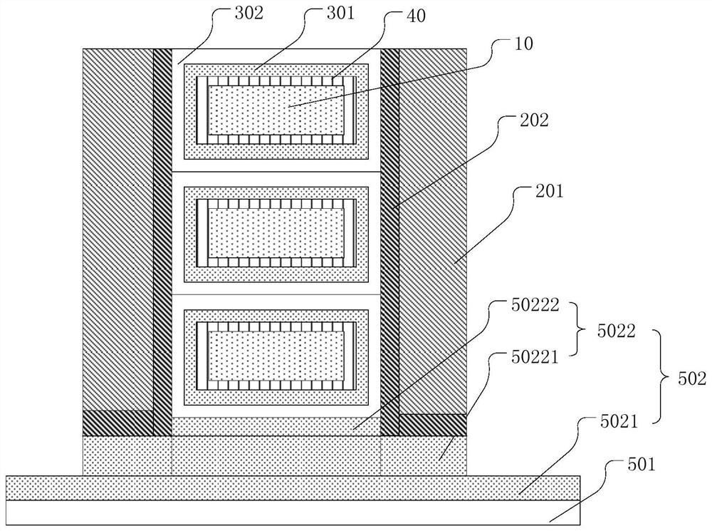
[0089] In order to solve the technical problems in the prior art that the internal wall technology has complicated procedures and high manufacturing difficulty, and the internal wall technology will also lead to an increase in the production cost of the gate-all-around device. The embodiment of the present invention discloses a semiconductor device, referring to figure 1 or figure 2 ,in, figure 1 A schematic structural diagram of a semiconductor device is shown, figure 2 It also shows a schematic structural dia...


PUM

PropertyMeasurementUnit
thicknessaaaaaaaaaa
thicknessaaaaaaaaaa
heightaaaaaaaaaa

Abstract

The invention discloses a semiconductor device and a manufacturing method thereof, an integrated circuit and an electronic device, and relates to the technical field of semiconductors. The invention aims to provide a semiconductor device which is simple in technology, low in manufacturing difficulty, low in production cost and capable of preventing transverse corrosion to a source-drain layer whennanowires are released. The semiconductor device includes: a gate-all-around transistor; wherein the gate-all-around transistor comprises a channel layer and a source-drain structure connected with the channel layer; a source-drain structure, the source-drain structure comprising a source-drain layer and a liner layer, and the liner layer being formed between the source-drain layer and the channel layer; the material of the liner layer being the same as that of the channel layer; or the absolute value of the difference between the mass percent of the target element contained in the material of the liner layer and the mass percent of the target element contained in the channel layer is smaller than the first threshold value.

Description

technical field [0001] The invention relates to the technical field of semiconductors, in particular to a semiconductor device, a manufacturing method thereof, an integrated circuit and electronic equipment. Background technique [0002] Stacked nanowire or sheet-ring-gate device is a new kind of semiconductor transistor, which has good gate control ability, can increase operating current and reduce short channel effect, so it has broad application prospects. [0003] The release of stacked nanowires / sheets is one of the key technologies to realize the integration of gate-all-around devices. At present, the inner wall technology is generally used to prevent the lateral corrosion of the source and drain layers when the nanowires are released. However, the internal wall technology has complex procedures and high manufacturing difficulty, which will also increase the production cost of the gate-all-around device. Contents of the invention [0004] The purpose of the present ...

Claims


Application Information

Patent Timeline
Patent Type & Authority Applications(China)
IPC IPC(8): H01L29/78H01L21/336H01L29/423H01L29/06
CPCH01L29/0603H01L29/0669H01L29/42356H01L29/66477H01L29/78
Inventor 李永亮昝颖程晓红李俊杰王文武
Owner INST OF MICROELECTRONICS CHINESE ACAD OF SCI
Why Eureka
Try Eureka