Technological method for etching tungsten gate

A process method and reactive gas technology, applied in the field of etching tungsten gates, can solve the problems affecting product yield, residual polysilicon layer, and large etching process, so as to remove silicide residues, improve selection ratio, and improve product quality. rate effect

Inactive Publication Date: 2009-09-16
BEIJING NAURA MICROELECTRONICS EQUIP CO LTD
View PDF0 Cites 6 Cited by
  • Summary
  • Abstract
  • Description
  • Claims
  • Application Information

AI Technical Summary

Problems solved by technology

However, the greater the thickness of the tungsten silicide layer / tungsten layer, the greater the difficulty of the etching process. If the selection ratio of the tungsten silicide layer / tungsten layer to the polysilicon layer is not high enough, it will inevitably lead to the tungsten silicide layer / tungsten layer. The remaining tungsten-containing components during the etching process (such as figure 1 As shown), this will affect the interface between the tungsten silicide layer / tungsten layer and the polysilicon layer, resulting in the polysilicon layer being blocked by the remaining tungsten-containing components and remaining, thus affecting the yield of the product

Method used


Image

  • Technological method for etching tungsten gate
  • Technological method for etching tungsten gate

Examples


Embodiment Construction

[0026] In order to make the objectives, technical solutions and advantages of the present invention clearer, the embodiments of the present invention will be described in further detail below in conjunction with the accompanying drawings.

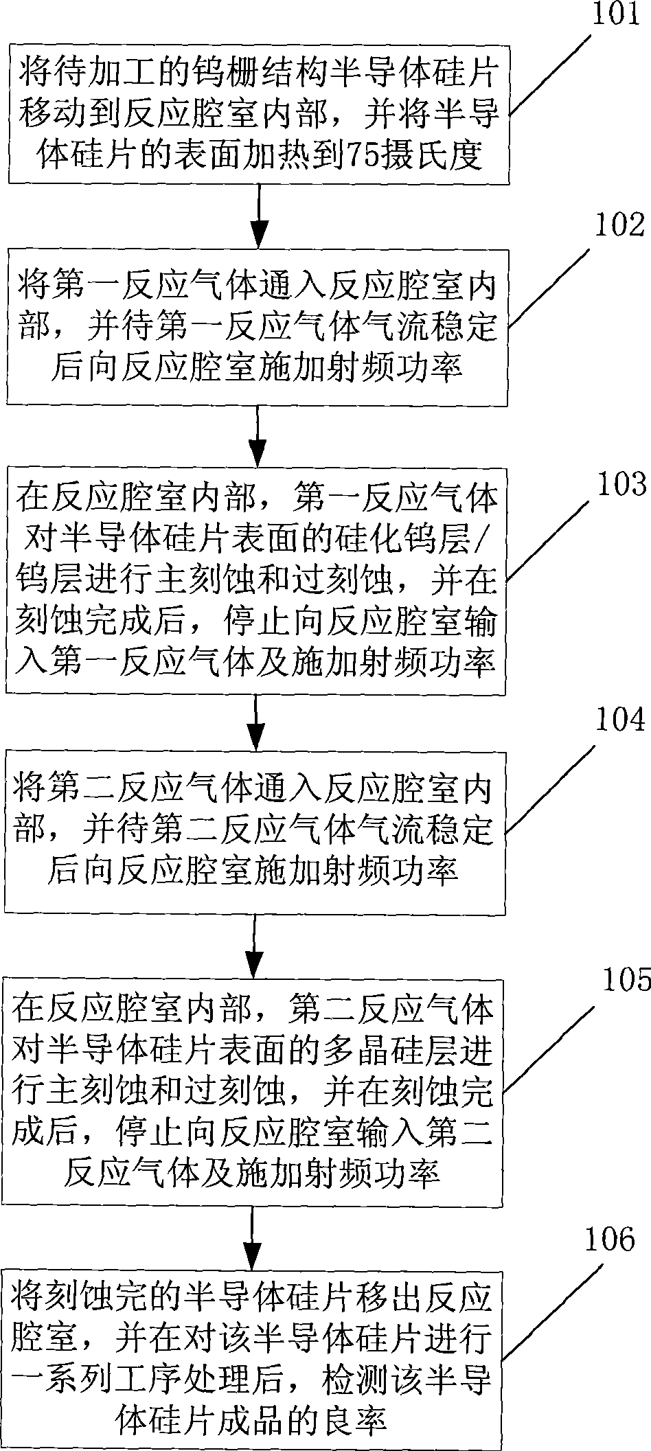
[0027] The technical solution provided by the embodiment of the present invention is different from the prior art in that: the embodiment of the present invention heats the surface of the semiconductor silicon wafer with a tungsten gate structure to be processed to a high temperature, and etches the semiconductor silicon wafer in the high temperature environment . The following takes heating the surface temperature of a semiconductor silicon wafer with a tungsten gate structure to 75 degrees Celsius as an example to illustrate the technical solutions provided by the embodiments of the present invention.

[0028] See figure 2 , The process method for etching a tungsten gate provided by an embodiment of the present invention specifically includes...


PUM


Abstract

The invention discloses a technological method for etching tungsten gate, pertaining to the field of semiconductor processing and manufacturing; the method comprises the following steps: a semiconductor silicon wafer is moved into a reaction chamber and heated to a high temperature; a first reaction gas is pumped into the reaction chamber; radio frequency power is imposed on the reaction chamber after the airflow of the first reaction gas becomes stable; and then, the first reaction gas etches the tungsten silicide layer or tungsten layer of the semiconductor silicon wafer; after the etching is finished, the pumping of the first reaction gas and the imposing of the radio frequency power are stopped; a second reaction gas is pumped into the reaction chamber; the radio frequency power is imposed on the reaction chamber after the airflow of the second reaction gas becomes stable; the second reaction gas etches the polysilicon layer of the semiconductor silicon wafer; after the etching is finished, the pumping of the second reaction gas and the imposing of the radio frequency power are stooped; and the semiconductor silicon wafer is moved out of the reaction chamber. The technological method improves the selection ratio between the tungsten silicide layer or tungsten layer and the polysilicon layer in the tungsten gate etching technology.

Description

Technical field [0001] The invention relates to the field of semiconductor processing and manufacturing, in particular to a process method for etching a tungsten gate. Background technique [0002] In the process of processing large-scale integrated circuits in the semiconductor industry, it is usually necessary to process fine-scale patterns on the surface of the silicon wafer. Among them, the tungsten gate etching process is widely used in the manufacture of memory chips or flash disk chips. The tungsten gate structure is generally divided into multiple layers, mainly including tungsten silicide layer / tungsten layer and polysilicon layer, etc. The thickness of the tungsten silicide layer determines the size of the storage space of the memory chip or flash memory chip. The more commonly used etching method for the tungsten gate etching process is distributed etching, that is, the tungsten silicide layer / tungsten layer is completed in two steps of main etching and over etching, a...

Claims


Application Information

Patent Timeline
Patent Type & Authority Applications(China)
IPC IPC(8): H01L21/28H01L21/3213H01L21/3065
Inventor 王娜
Owner BEIJING NAURA MICROELECTRONICS EQUIP CO LTD
Why Eureka
Try Eureka