Device for gas linear cutting of silicon slice

A wire cutting and gas technology, applied in the direction of electrical components, semiconductor/solid-state device manufacturing, film technology, etc., can solve the problems of difficult control of cutting line width, low positioning accuracy, rough cutting section, etc., and achieve high etching rate Fast, simple equipment, high cross-section smoothness

Inactive Publication Date: 2010-11-10
INST OF MICROELECTRONICS CHINESE ACAD OF SCI
View PDF0 Cites 5 Cited by
  • Summary
  • Abstract
  • Description
  • Claims
  • Application Information

AI Technical Summary

Problems solved by technology

Although this method is simple and practical, and the cutting speed is fast, this cutting method must be accompanied by high-pressure water flow for cooling and cleaning, the pressure and torque generated by the contact between the dicing knife and the silicon wafer, and the impact of the cut silicon chips on the surface. Deadly Hazards Caused by Chips
The positioning accuracy of this cutting machine is not high, and due to the thickness of the blade, it is difficult to control the cutting line width
Although the new laser cutting technology overcomes some problems existing in the traditional cutting technology, it also has the disadvantages of rough cutting section and expensive equipment.

Method used


Image

  • Device for gas linear cutting of silicon slice
  • Device for gas linear cutting of silicon slice
  • Device for gas linear cutting of silicon slice

Examples


Embodiment Construction

[0020] In order to make the object, technical solution and advantages of the present invention clearer, the present invention will be described in further detail below in conjunction with specific embodiments and with reference to the accompanying drawings.

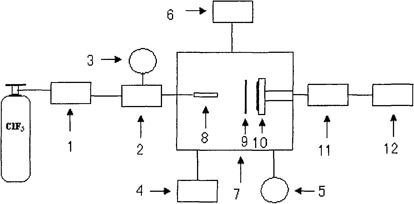
[0021] The invention uses chlorine trifluoride as an etching reaction gas to cut and process silicon wafers, which can well solve the problems existing in the traditional technology. Chlorine trifluoride cutting silicon wafers is carried out in a plasma-free environment, the etching rate of silicon is fast, the steepness and smoothness of the side walls are greatly improved, and the silicon wafer wire cutting equipment is simple, easy to implement and popularize .

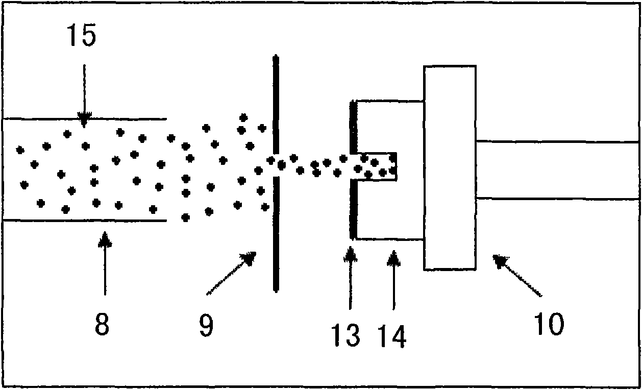
[0022] Such as figure 1 as shown, figure 1 It is a structural schematic diagram of a device for gas wire cutting of silicon wafers provided by the present invention, which includes a flow controller 1, a pressure reducing valve 2, a pressure gauge 3, a vacuu...


PUM


Abstract

The invention discloses a device for the gas linear cutting of a silicon slice, which comprises a flow controller, a pressure reducing valve, a pressure gauge, a vacuum pump, a vacuum-cavity pressure gauge, a vacuum-cavity temperature control device, a vacuum chamber, a spray head, a masking plate, a silicon slice frame, a post pump and a tail gas processing device, wherein the pressure reducing valve, the vacuum pump, the vacuum-cavity pressure gauge, the vacuum-cavity temperature control device and the post pump are respectively connected with the vacuum chamber, gas enters the vacuum chamber after sequentially passing through the flow controller, the pressure reducing valve and the spray head, then the silicon slice on the silicon slice frame is cut through the masking and the beam convergence and regulation of the masking plate, the temperature of the vacuum chamber is controlled to be under a room temperature environment through the vacuum-cavity temperature control device, and etched tail gas is pumped out of the vacuum chamber through the post pump and enters the tail gas processing device through the post pump. In the invention, chlorine trifluoride is used as etching reaction gas for carrying out cutting processing for the silicon slice, and the problems existing in a traditional technology can be well solved.

Description

technical field [0001] The invention relates to the technical field of silicon wafer cutting in semiconductor technology, in particular to a device for gas wire cutting of silicon wafers. Background technique [0002] With the extension of IC manufacturing to smaller process nodes and complex processes, as well as the unique complex structure of MEMS chips, the traditional silicon wafer cutting technology can no longer meet the requirements of the development of semiconductor manufacturing technology. [0003] Traditional silicon wafer cutting (scribing) is generally achieved by high-speed rotation of the scribing wheel. Although this method is simple and practical, and the cutting speed is fast, this cutting method must be accompanied by high-pressure water flow for cooling and cleaning, the pressure and torque generated by the contact between the dicing knife and the silicon wafer, and the impact of the cut silicon chips on the surface. Deadly hazards posed by chips. The...

Claims


Application Information

Patent Timeline
Patent Type & Authority Applications(China)
IPC IPC(8): C23F1/08H01L21/78B81C5/00
Inventor 景玉鹏惠瑜
Owner INST OF MICROELECTRONICS CHINESE ACAD OF SCI
Why Eureka
Try Eureka