Solar cell and manufacturing method thereof

A solar cell and manufacturing method technology, applied in circuits, electrical components, photovoltaic power generation and other directions, can solve the problems of difficult manufacturing process and low efficiency, etc.

CN112885924APending Publication Date: 2021-06-01LONGI SOLAR TECH (TAIZHOU) CO LTD
12 Cites 3 Cited by

Patent Information

Authority / Receiving Office
CN · China
Patent Type
Applications(China)
Current Assignee / Owner
Publication Date
2021-06-01

Smart Images

  • Figure 1
    Figure 1
  • Figure 2
    Figure 2
  • Figure 3
    Figure 3
Patent Text Reader

Abstract

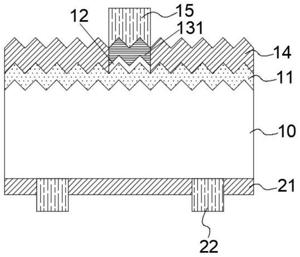
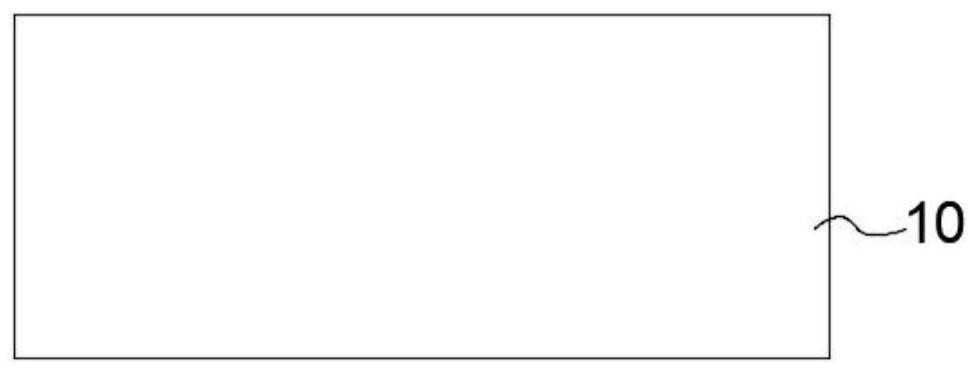
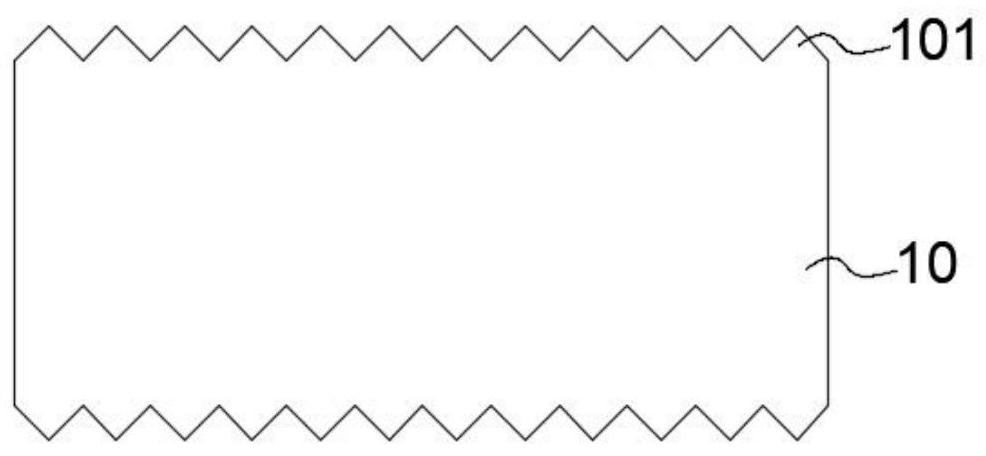
The invention discloses a solar cell and a manufacturing method thereof, relates to the technical field of photovoltaics, and aims to reduce the manufacturing difficulty of a local passivation contact structure and improve the manufacturing efficiency. The manufacturing method of the solar cell comprises the following steps of: providing a silicon substrate; forming a tunneling layer on the front surface of the silicon substrate; forming an amorphous silicon layer on the tunneling layer; processing the target part of the amorphous silicon layer to form a doped polycrystalline silicon region and an amorphous silicon region; and removing the amorphous silicon region to obtain a local passivation contact structure on the front surface of the silicon substrate. The solar cell is manufactured by adopting the manufacturing method of the solar cell. The solar cell and the manufacturing method thereof provided by the invention are used for solar cell manufacturing.
Need to check novelty before this filing date? Find Prior Art

Description

technical field

[0001] The invention relates to the field of photovoltaic technology, in particular to a solar cell and a manufacturing method thereof. Background technique

[0002] With the continuous development of photovoltaic technology, crystalline silicon solar cell technology is becoming more and more mature, and its conversion efficiency is constantly approaching the theoretical limit. At present, the main factor affecting the open circuit voltage and conversion efficiency of crystalline silicon solar cells is the carrier recombination in the contact area between the metal electrode and the crystalline silicon surface.

[0003] In order to reduce carrier recombination in the contact area between the metal electrode on the front of the solar cell and the crystalline silicon surface, a local passivation contact structure can be made in the area where the crystalline silicon surface contacts the metal electrode. However, the manufacturing process of the local passivati...

Examples

Embodiment Construction

[0033] In order to clearly describe the technical solutions of the embodiments of the present invention, in the embodiments of the present invention, words such as "first" and "second" are used to distinguish the same or similar items with basically the same function and effect. Those skilled in the art can understand that words such as "first" and "second" do not limit the number and execution order, and words such as "first" and "second" do not necessarily limit the difference.

[0034] It should be noted that, in the present invention, words such as "exemplary" or "for example" are used as examples, illustrations or illustrations. Any embodiment or design described herein as "exemplary" or "for example" should not be construed as being preferred or advantageous over other embodiments or designs. Rather, the use of words such as "exemplary" or "such as" is intended to present related concepts in a concrete manner.

[0035] In the present invention, "at least one" means one ...