Preparation method of patterned composite substrate

A composite substrate and patterning technology, applied in electrical components, circuits, semiconductor devices, etc., can solve the problems of LED chip photoelectric performance impact, LED chip edge area damage, limiting LED internal quantum efficiency, etc., to improve the LED internal quantum efficiency. Efficiency, avoid high chip rejection rate, avoid the effect of LED light-emitting area damage

Inactive Publication Date: 2019-06-04
江苏澳洋顺昌集成电路有限公司
View PDF5 Cites 4 Cited by
  • Summary
  • Abstract
  • Description
  • Claims
  • Application Information

AI Technical Summary

Problems solved by technology

However, the difference between the refractive index of sapphire (n≈1.78) and the refractive index of GaN material (n≈2.5) is only about 0.7, which is not conducive to further improving the light extraction efficiency of LEDs; at the same time, factors such as the large lattice mismatch between PSS itself and GaN Limits the further improvement of quantum efficiency in LED
In addition, due to the large chemical bond energy and stable performance of sapphire materials, it is difficult to prepare PSS and the cost is high.
In addition, in the process of LED chip processing, when the wafer is divided into LED chip units by using ultraviolet laser cutting method, the laser ablation will damage the edge area of ​​the LED chip and affect the electrical performance; in addition, the residue generated during the cutting process falls on the chip. The surface is not easy to clean, which affects the light extraction efficiency
In particular, for small-sized chips such as Mini-LED and Micro-LED, if laser cutting is still used for chip separation, the damage ratio of the chip area will be relatively large, and the effective light-emitting area will be reduced, which will inevitably affect the photoelectric performance of the LED chip. Serious impact, and reduced yield during mass production

Method used


Image

  • Preparation method of patterned composite substrate
  • Preparation method of patterned composite substrate
  • Preparation method of patterned composite substrate

Examples


Embodiment 1

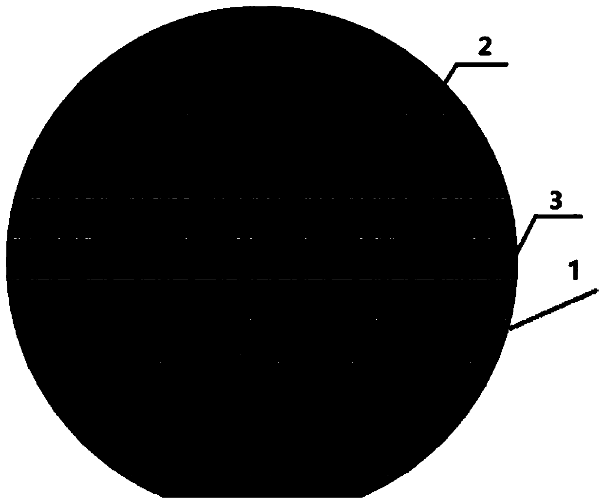
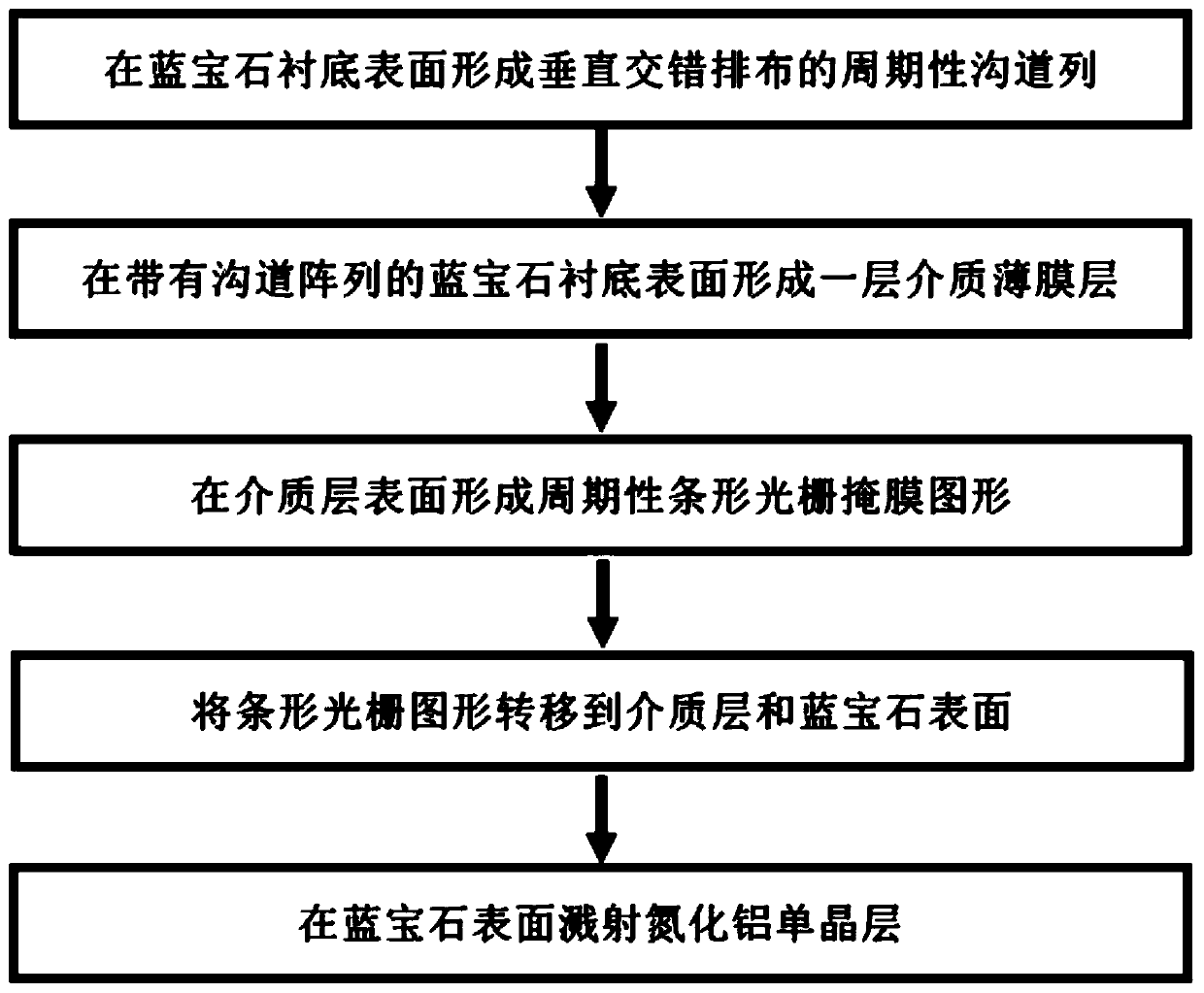
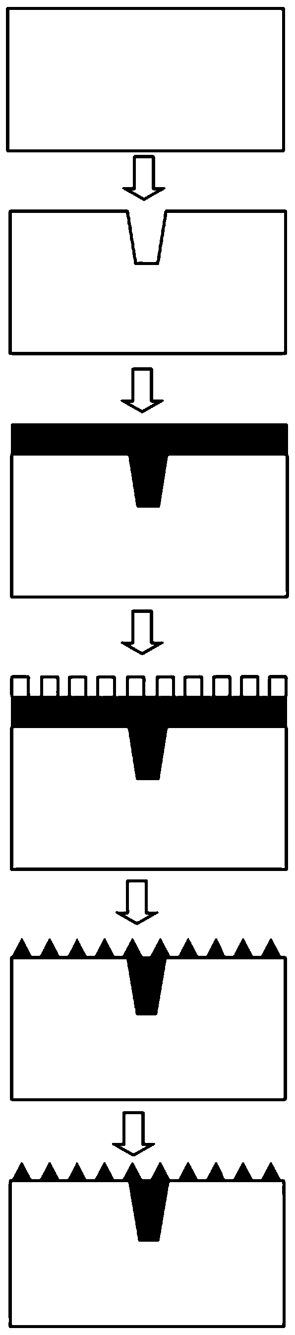
[0029] like figure 1 , 2 , 3 and 4, the present invention discloses a method for preparing a patterned sapphire substrate, comprising the following steps:

[0030] Step 1: put the sapphire substrate 1 into a laser cutting machine for cutting, and form a periodic channel array with several channels 3 arranged alternately on the surface of the sapphire substrate 1 . The angle between the horizontal and vertical channels is 90°, the period of the horizontal and vertical channels is 10μm-1000μm, the channel width is 10μm-50μm, the channel depth is 40μm-120μm, and the slope of the channel side wall is 30° -90°. For example, it can be specifically: the periodic distribution of the lateral and vertical channels is 10 μm, 100 μm, 500 μm or 1000 μm, the channel width is 10 μm, 20 μm, 30 μm or 50 μm, and the slope of the channel side wall is 40°, 60° or 90° . The specific number can also be flexibly selected within the above range.

[0031] Step 2: Deposit a layer of dielectric fil...


PUM

PropertyMeasurementUnit
thicknessaaaaaaaaaa
thicknessaaaaaaaaaa
thicknessaaaaaaaaaa

Abstract

The invention provides a preparation method of a patterned composite substrate. The preparation method comprises the steps of: step 1, placing a sapphire substrate on a laser cutting machine for cutting, and forming a plurality of periodic channel arrays which are arranged in a vertically staggered manner on the surface of the sapphire substrate; step 2, realizing a dielectric thin film layer on the surface of the cleaned sapphire substrate; step 3, forming a periodic strip grating mask pattern on the sapphire substrate provided with the dielectric thin film layer; step 4, and transferring themask pattern onto the dielectric thin film layer and the sapphire substrate, wherein a strip-shaped grating microstructure pattern is formed on the surface of the sapphire substrate, forming a aluminum nitride single crystal thin film layer on the surface after cleaning the sapphire substrate, and finally realizing the patterned composite substrate. The preparation method effectively avoids the problem of photoelectric performance damage of an LED chip, greatly improves the luminous efficiency of the LED chip, improves the process yield and reduces the production cost.

Description

technical field [0001] The invention relates to a patterned composite substrate, in particular to a method for preparing a patterned composite substrate mainly used in the epitaxy of high-efficiency GaN-based light-emitting diodes (GaN-based LED). Background technique [0002] The third-generation semiconductor materials mainly consist of gallium nitride (GaN), aluminum nitride (AlN), indium nitride (InN) and their ternary and quaternary alloy materials, because their energy band width can range from 0.7eV to 6.2eV is continuously adjustable, and both are direct bandgap, and its excellent physical and chemical stability, high saturation electron mobility and other characteristics make it the first choice for GaN-based light-emitting diodes (LEDs), lasers, electronic power devices and other optoelectronic devices Material. However, because it is very difficult to prepare GaN single crystal materials, and it is difficult to find substrate materials that match the GaN lattice,...

Claims


Application Information

Patent Timeline
Patent Type & Authority Applications(China)
IPC IPC(8): H01L33/00H01L33/20H01L33/44H01L33/12
Inventor 刘坚
Owner 江苏澳洋顺昌集成电路有限公司
Why Eureka
Try Eureka