Improved memory cell for silicon static state stochastic memory of part depletion isolator

A storage unit, static random technology, applied in the direction of electric solid state devices, semiconductor devices, electrical components, etc., can solve the problems of increasing the static power consumption of the chip, increasing the leakage current, and the power consumption of the latch-up effect, so as to avoid the floating body effect and reduce the power consumption. The effect of simplifying power consumption and wiring

Inactive Publication Date: 2009-05-27
INST OF SEMICONDUCTORS - CHINESE ACAD OF SCI
View PDF1 Cites 2 Cited by
  • Summary
  • Abstract
  • Description
  • Claims
  • Application Information

AI Technical Summary

Problems solved by technology

The former has a small unit area and is easy to obtain a memory with a large integration level, but it is prone to latch-up effect and consumes a lot of power; the latter can completely avoid the latch-up effect due to well-known reasons and consumes less power. If it can be better Solve the problem caused by the body area, and can also suppress the "floating body effect", and the performance of PDSOI SRAM in the radiation environment is much better than that of bulk silicon CMOS SRAM
[0005] A kind of PDSOI SRAM (see figure 2 ), the load PMOS transistor and the access NMOS transistor both adopt a T-shaped gate body contact structure. Due to the "island effect" of the T-shaped gate, it will increase leakage, especially after irradiation, it is more likely to cause additional leakage current and increase Static power consumption of the chip

Method used


Image

  • Improved memory cell for silicon static state stochastic memory of part depletion isolator
  • Improved memory cell for silicon static state stochastic memory of part depletion isolator
  • Improved memory cell for silicon static state stochastic memory of part depletion isolator

Examples


Embodiment Construction

[0026] The content of the present invention is described in detail below through the accompanying drawings, so that the features and advantages of the present invention become clearer. These drawings include:

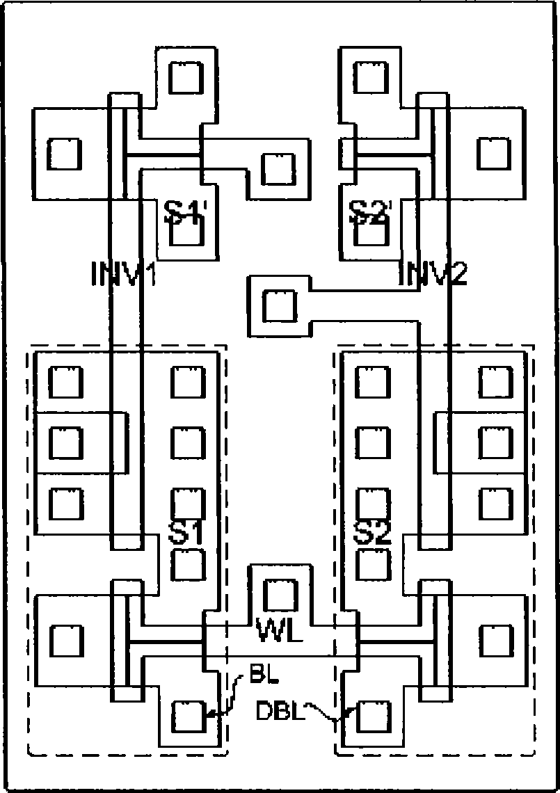
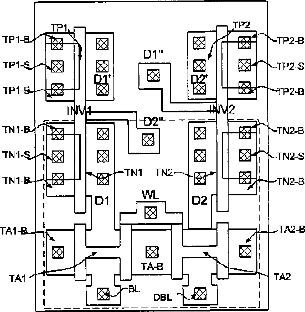
[0027] image 3 Shown is the improved PDSOI six-transistor memory cell of the present invention, attention should be paid to the body extraction method of the six transistors, especially the H-type gate body extraction structure used for accessing NMOS transistors.

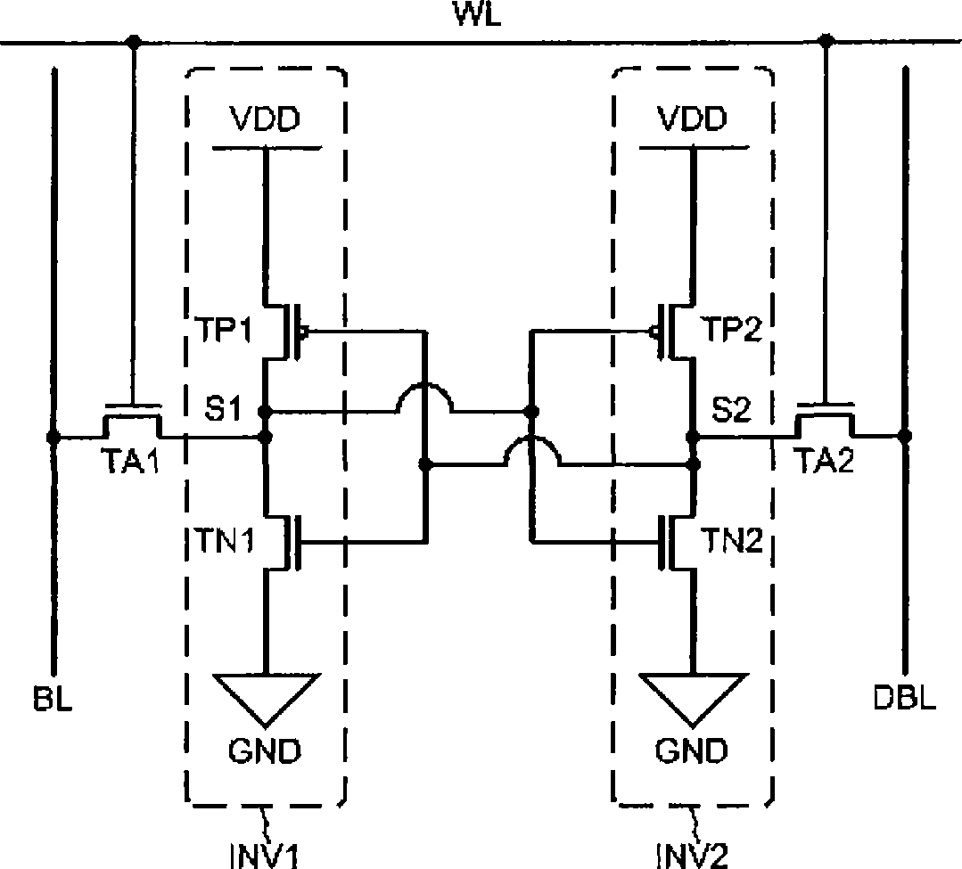
[0028] Figure 4 Shown is image 3 In the circuit connection diagram of the SRAM unit of the present invention, the body region of each transistor is connected to a corresponding fixed potential.

[0029] As shown in the figure, a CMOS SRAM cell with six transistors formed on a partially-depleted (PD) silicon-on-insulator (SOI) substrate.

[0030] The unit is implemented on a partially depleted silicon-on-insulator (PDSOI) substrate, and the six transistors are all subjected to body contact processing. A...


PUM


Abstract

The invention provides a storage unit for improving a static random access memory formed on a partially depleted SOI substrate, which relates to the technology of the static random access memory. The SRAM unit comprises six transistors, namely a first access NMOS transistor, a second access NMOS transistor, a first drive NMOS transistor, a second drive NMOS transistor, a first load PMOS transistor and a second load PMOS transistor. When body-area contact processing is carried out, T-type gate technology is not adopted, the NMOS transistors are accessed by an H-type gate body contact, and the load PMOS transistors and the drive NMOS adopt BTS-A type gate body contact. Therefore, not only floating body effect caused by the partially depleted SOI material can be avoided, but also island side creepage caused by a T-type gate structure can be inhibited. Two groups of inverters in the unit are linked in the middle of the unit so as to simplify cabling and reduce area of the unit. The storage unit improves the final performance of a chip.

Description

technical field [0001] The invention relates to the technical field of static random access memory (SRAM), more specifically, an improved partially depleted silicon-on-insulator SRAM storage unit, which is used for partially depleting silicon-on-insulator (PDSOI, Partial Depleted Silicon on Insulator, ) SRAM on the substrate. Background technique [0002] According to the data storage method, semiconductor memory is divided into dynamic random access memory (DRAM), non-volatile memory and static random access memory (SRAM). SRAM has established its unique advantage by being able to achieve fast operating speeds in a simple and low power consumption manner. Also, compared to DRAM, SRAM is relatively easy to design and manufacture because it does not need to periodically refresh the stored information. [0003] See figure 1 , usually, an SRAM cell consists of two drive transistors, two load devices, and two access transistors. According to the type of load device contained...

Claims


Application Information

Patent Timeline
Patent Type & Authority Applications(China)
IPC IPC(8): H01L27/12H01L23/528
Inventor 赵凯刘忠立于芳
Owner INST OF SEMICONDUCTORS - CHINESE ACAD OF SCI
Why Eureka
Try Eureka