Semiconductor package having marking layer
A semiconductor and mold cavity technology, which is applied in semiconductor devices, semiconductor/solid-state device manufacturing, semiconductor/solid-state device components, etc., can solve the problem of unacceptable failure rate of ultra-thin devices, and achieve the effect of maintaining accurate thinness
- Summary
- Abstract
- Description
- Claims
- Application Information
AI Technical Summary
Problems solved by technology
Method used
Image

Examples
Embodiment Construction
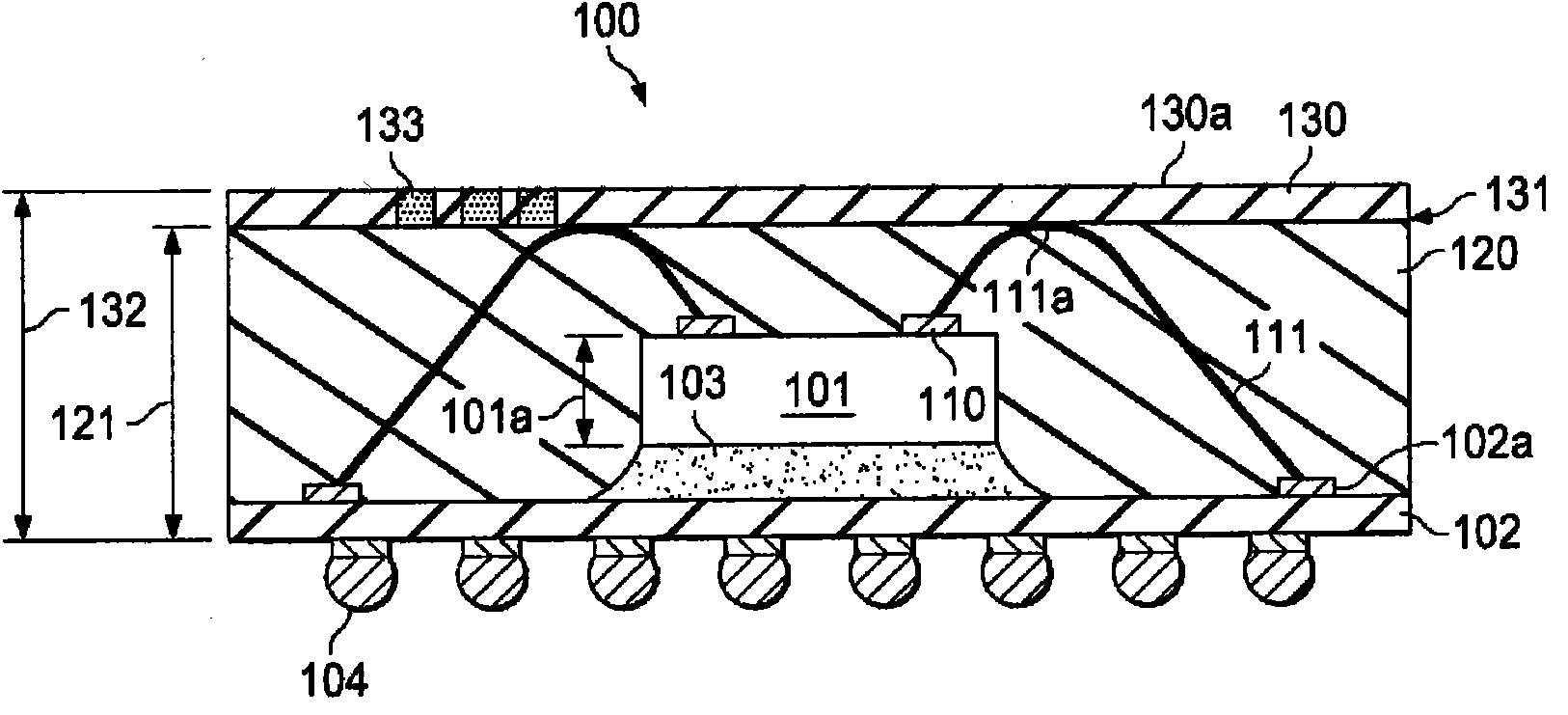
[0027] figure 1 A semiconductor device generally designated 100 is shown as an embodiment of the invention. The assembled semiconductor chip 101 is encapsulated in a polymer compound 120 . On the top surface of the compound 120 is a sheet 130, preferably made of a polymeric material (see below), attached to the encapsulating compound 120 and in continuous contact with said compound. The sheet 130 has a bare and generally flat surface 130a. Such as figure 1 As indicated, the encapsulating compound shares a boundary 131 with the sheet 130 .
[0028]The polymeric material of flake 130 is selected to provide a flake having a first optical reflectivity and a first color. When a pulse of energy, such as a pulse of focused laser light, or another high-intensity light source impinges on a spot 133 of the sheet 130, the energy is absorbed by the material of the spot (primarily as thermal energy), thereby increasing the temperature. The polymeric material locally alters its chemic...
PUM
 Abstract
Description
Claims
Application Information
 - R&D
- Intellectual Property
- Life Sciences
- Materials
- Tech Scout
- Unparalleled Data Quality
- Higher Quality Content
- 60% Fewer Hallucinations
Browse by: Latest US Patents, China's latest patents, Technical Efficacy Thesaurus, Application Domain, Technology Topic, Popular Technical Reports.
© 2025 PatSnap. All rights reserved.Legal|Privacy policy|Modern Slavery Act Transparency Statement|Sitemap|About US| Contact US: help@patsnap.com