Single-side double contact flexible circuit board and making method thereof

A flexible circuit board, single-sided double-contact technology, applied in the direction of printed circuit manufacturing, printed circuit, printed circuit components, etc., can solve problems such as wrinkle deformation, affecting product yield, fracture, etc.

Active Publication Date: 2011-01-05
XIAMEN HONGXIN ELECTRON TECH
View PDF5 Cites 17 Cited by
  • Summary
  • Abstract
  • Description
  • Claims
  • Application Information

AI Technical Summary

Problems solved by technology

[0004] However, the gold finger 6 of the single-sided double-contact flexible circuit board produced by this process is in a suspended state, so in the production proce...

Method used


Image

  • Single-side double contact flexible circuit board and making method thereof
  • Single-side double contact flexible circuit board and making method thereof
  • Single-side double contact flexible circuit board and making method thereof

Examples


Embodiment Construction

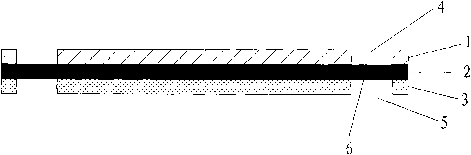
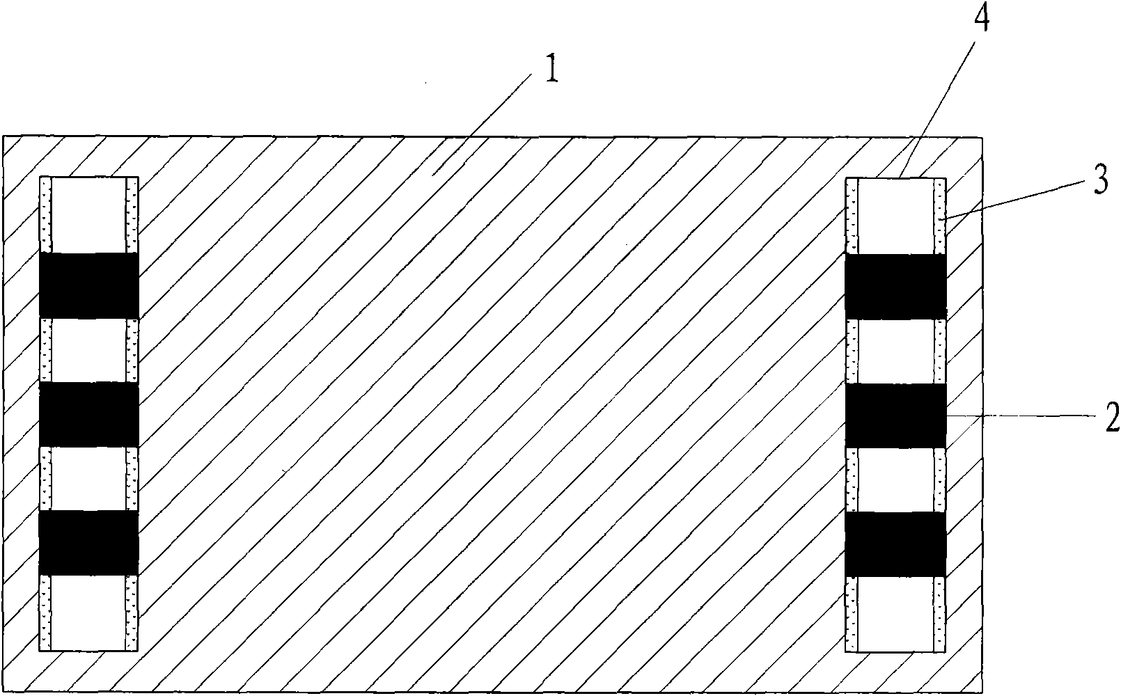
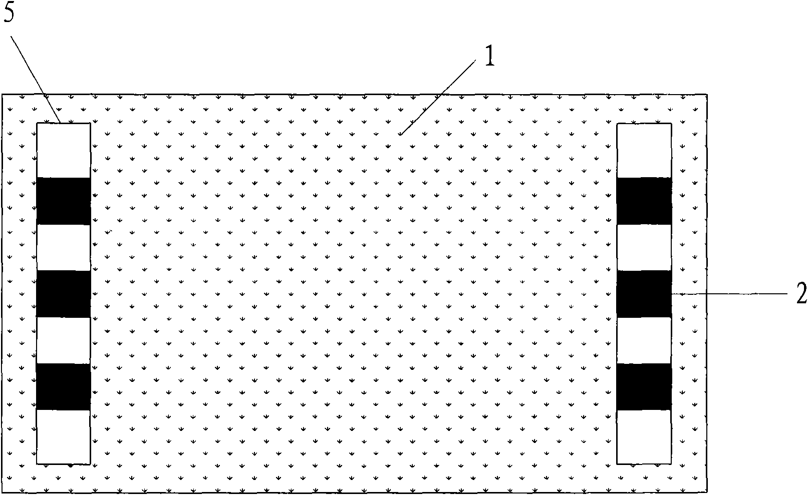
[0024] Such as Figure 5 , Figure 6 , Figure 7 As shown, a single-sided double-contact flexible circuit board disclosed by the present invention includes a base material layer 30, a copper foil layer 20, and a cover film 10. The base material layer 30 and the cover film 10 are respectively provided with a bottom base material opening 50 and a cover film 10. Openings 40 in the top cover film to form gold fingers 60 that can be in contact with the outside world on both sides; the openings 50 of the bottom substrate are spaced apart from the corresponding gold fingers 60, and the size of each bottom substrate opening 50 is smaller than the size of the top cover film 10 finger area .

[0025] Cooperate Figure 8 As shown, the single-sided double-contact flexible circuit board of the present invention and its manufacturing method specifically include the following steps:

[0026] (1) Cutting: Cut the materials used according to the specifications and sizes required for produc...


PUM


Abstract

The invention discloses a single-side double contact flexible circuit board and a making method thereof. The single-side double contact flexible circuit board comprises a substrate layer, a copper foil layer and a covering film layer, wherein the substrate layer and the copper foil layer are both a single-side copper clad board. The making method comprises the following steps of: firstly, blanking, making a line on a copper foil surface of the single-side copper clad board, adhering a covering film with a drill hole and a punched opening on a covering film at the top layer, laminating and curing; secondly, laser-cutting an opening of a substrate at the bottom layer on the substrate surface of the single-side copper clad board with the made line, wherein the opening size of the substrate at the bottom layer is a little less than the size of a finger area of the covering film at the top layer; thirdly, removing a foreign body at a bare copper part of a product by adopting modes of plasma treatment and surface treatment; and fourthly, carrying out procedures of surface coating, character screen printing, electric measurement and punching forming to obtain the single-side double contact flexible circuit board, and therefore, the periphery of a golden finger is supported by the copper clad board substrate at the bottom layer, the buckling deformation resistance capacity of the golden finger in the production process and the subsequent use process is strengthened, the product making yield rate is enhanced, the cost waste is reduced, and the circuit board has the advantages of simple structure and good performance.

Description

technical field [0001] The invention relates to a flexible circuit board and a manufacturing method thereof, in particular to a single-sided double-contact flexible circuit board and a manufacturing method thereof. Background technique [0002] With the miniaturization and lightweight development of various electronic equipment, it is required to use flexible circuit boards with thin thickness, light weight, superior bending performance and multi-functionality as important accessories of electronic equipment, single-sided flexible circuit boards Only the pad side can be connected to the electronic components. Although the double-sided flexible circuit board can be connected to the electronic components on both sides, the thickness of the socket end is relatively thick. Therefore, the single-sided double-contact flexible circuit board is thus produced. [0003] At present, the structure diagram of the commonly used single-sided double-contact flexible circuit board is as foll...

Claims


Application Information

Patent Timeline
IPC IPC(8): H05K1/02H05K3/00
Inventor 续振林陈妙芳
Owner XIAMEN HONGXIN ELECTRON TECH
Why Eureka
Try Eureka