

ESD protective circuit with control circuit for integrated circuit
An ESD protection, integrated circuit technology, applied in the field of electronics, can solve the problem of occupying the area of the silicon chip, and achieve the effect of reducing the trigger voltage and reducing the false trigger phenomenon.
- Summary
- Abstract
- Description
- Claims
- Application Information
AI Technical Summary
Problems solved by technology
Method used
Image

Examples
specific Embodiment approach 1
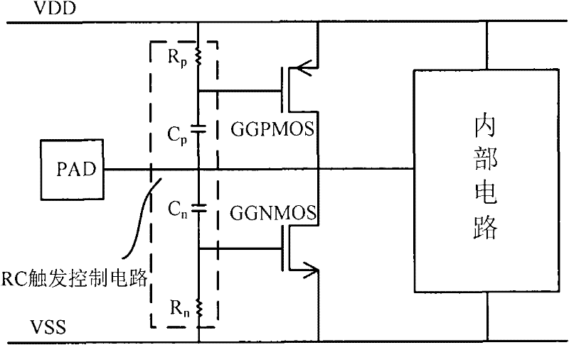
[0024] An ESD protection circuit with a control circuit for an integrated circuit, such as Figure 4As shown, it includes a control circuit 3 , a protection circuit 4 and an ESD power supply clamping circuit 6 . The control circuit 3 is composed of an RC trigger circuit 1 and an inverter group 2; the VDD rail in the dual rails of the integrated circuit power supply is connected in series with the VSS rail in the dual rails of the integrated circuit power supply through the RC trigger circuit 1 formed by series connection of a resistor R and a capacitor C ; The inverter group 2 is formed in series by the first-stage inverter 7 and the second-stage inverter 8; The input ends of the first-stage inverter 7 are connected, and the output end of the first-stage inverter 7 is connected with the input end of the second-stage inverter 8 . The protection circuit 4 is realized by complementary NMOS transistors and PMOS transistors, wherein a PMOS transistor is connected between each I / O ...
specific Embodiment approach 2
[0032] An ESD protection circuit with a control circuit for an integrated circuit, such as Figure 9 As shown, it includes a control circuit 3 , a protection circuit 4 and an ESD power supply clamping circuit 6 . The control circuit 3 is composed of an RC trigger circuit 1 and an inverter group 2; the VDD rail in the dual rails of the integrated circuit power supply is connected in series with the VSS rail in the dual rails of the integrated circuit power supply through the RC trigger circuit 1 formed by connecting the capacitor C and the resistor R in series ; The inverter group 2 is formed in series by the first-stage inverter 7 and the second-stage inverter 8; The input ends of the first-stage inverter 7 are connected, and the output end of the first-stage inverter 7 is connected with the input end of the second-stage inverter 8 . The protection circuit 4 is realized by complementary NMOS transistors and PMOS transistors, wherein a PMOS transistor is connected between each...
specific Embodiment approach 3
[0035] In the aforementioned two specific implementation methods, the number of stages of the inverter group can be increased from two stages to multiple stages, and the rest of the circuit structure remains unchanged, and the following can be obtained: Figure 10 The specific implementation shown. This particular embodiment increases the number of inverter stages in the inverter group 2, which can make the action of the trigger circuit faster when ESD occurs, but considering the area factor, the better choice is 3 or 4 , At the same time, the output of the last two stages of inverters should be reasonably selected, or the positions of R and C should be swapped to ensure correct level logic.
[0036] To sum up, the present invention provides a single control circuit to control a plurality of ESD protection circuit structure, which saves the silicon chip area occupied by the control circuit. At the same time, some auxiliary ESD discharge channels are provided outside the main ...
PUM
 Abstract
Description
Claims
Application Information