Method for repairing open circuit of thick copper lead wire and repairing structure thereof

A technology of copper wire and copper layer, which is applied in the direction of printed circuit, printed circuit manufacturing, conductive pattern reinforcement, etc., can solve the problems of poor appearance quality of printed boards, inability to repair thick copper wire disconnection, insufficient mechanical strength, etc., to achieve The effect of fast speed and meeting the requirements of appearance quality

Active Publication Date: 2011-12-21
福州瑞华印制线路板有限公司
View PDF0 Cites 0 Cited by
  • Summary
  • Abstract
  • Description
  • Claims
  • Application Information

AI Technical Summary

Problems solved by technology

[0002] There will be 1%-2% wire circuit boards in the reproduction process of printed circuit boards. Two methods can be used to repair such circuit boards. One is to use ordinary pressure welding to repair wire circuit breaks. There are three defects in this type of pressure welding. : 1. The solder joints are only on two pressure soldering points, resulting in no practical contact between the repaired copper wire and the base material at the gap of the printed circuit board, and the open circuit with a large span cannot be repaired; 2. Only small openings can be repaired There is nothing to do about broken wires and straight line wires, large-area wires and curved wires; 3. The appearance quality of the repaired printed board is poor
However, this chemical method cannot repair the defects of broken wires of thick copper wires, and there are problems such as insufficient mechanical strength.

Method used


Image

  • Method for repairing open circuit of thick copper lead wire and repairing structure thereof
  • Method for repairing open circuit of thick copper lead wire and repairing structure thereof
  • Method for repairing open circuit of thick copper lead wire and repairing structure thereof

Examples


Embodiment Construction

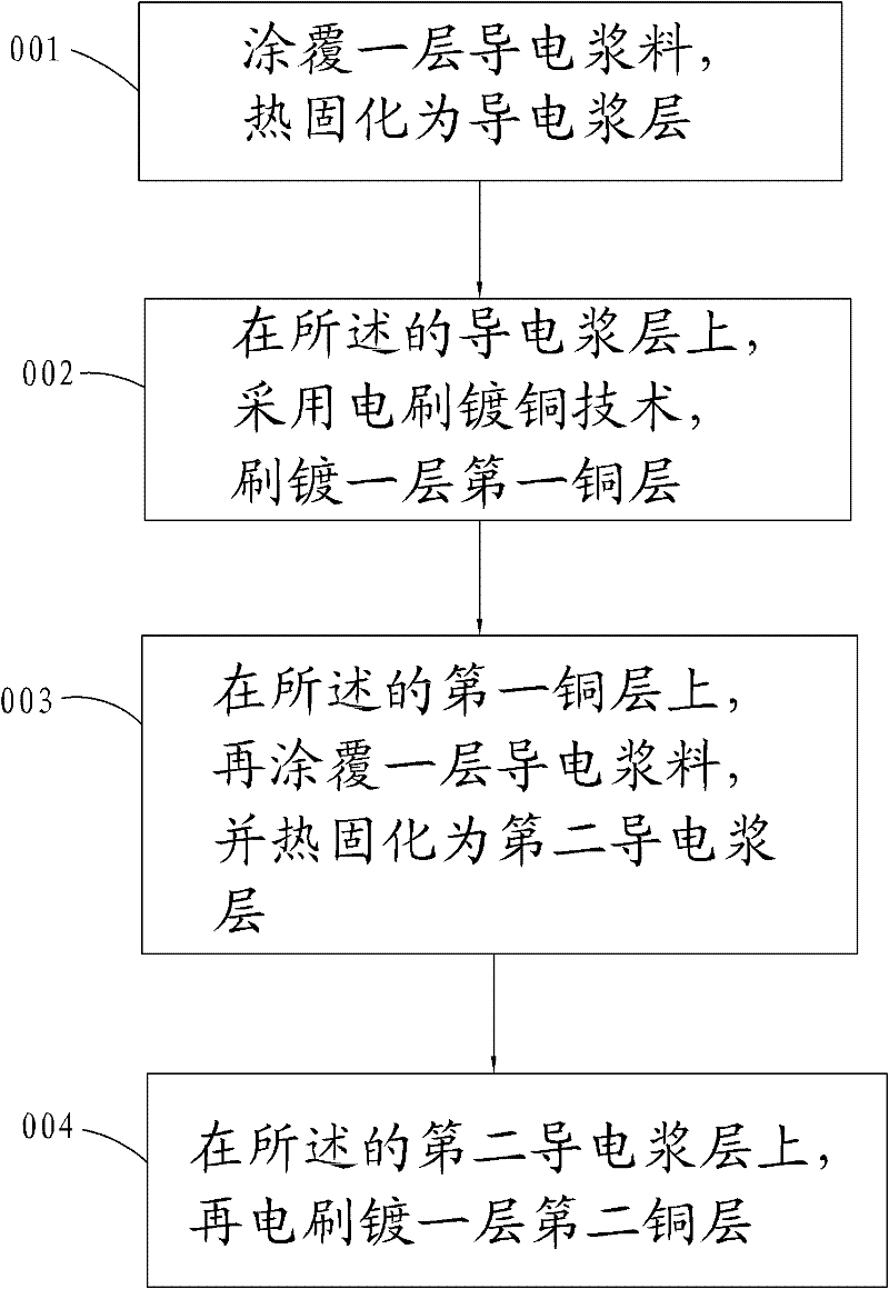
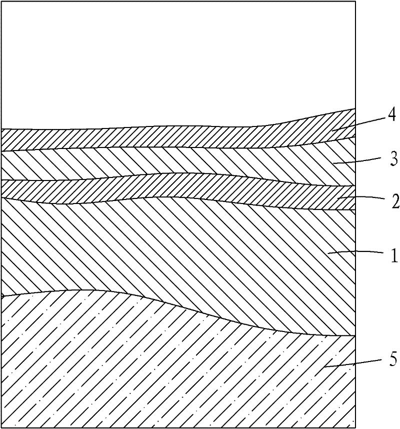
[0026] refer to figure 1 with figure 2 , the embodiment of the present invention will be described in detail.

[0027] Such as figure 1 , is an embodiment of a method for repairing a thick copper wire disconnection of the present invention. In the first step, at first, a layer of conductive paste is coated on the broken or incomplete position of the thick copper wire, and the conductive paste is silver paste. The silver paste is thermally cured to form a first silver paste layer, which serves as the basis for the conductive layer and subsequent repairs. The second step is to brush-plate a layer of first copper layer on the first silver paste layer. The first copper layer is a copper layer brush-plated with copper nitrate solution. The third step is to coat a layer of conductive paste on the first copper layer, the conductive paste is silver paste, and dry the silver paste to form the second silver paste layer. In the fourth step, a second copper layer is brush-plated on ...


PUM


Abstract

The invention provides a method for repairing the open circuit of a thick lead wire, which is based on the technology of conductive paste rendering and electric brush plating. The method comprises the following steps of: 001, coating a layer of conductive paste at the position to be repaired, wherein the conductive paste is thermally cured into a first conductive paste layer; 002, playing a first copper layer on the first conductive paste layer by adopting the electric brush plating technology; 003, coating one more conductive paste layer on the first copper layer, wherein the conductive paste layer is thermally cured into a second conductive paste layer; and 004, plating a second copper layer on the second conductive paste layer by adopting the electric brush plating technology. The invention provides a repairing structure adopting the method for repairing the open circuit of the thick copper lead wire, which comprises the first conductive paste layer, the first copper layer, the second conductive paste layer and the second copper layer from the inside to the outside. The invention not only overcomes the defect of the conventional pressure welding, but also meets the requirements on the mechanical strength and electric performance of the repaired position.

Description

【Technical field】 [0001] The invention relates to a technology for repairing circuit breaks in printed circuit boards, in particular to a method for repairing circuit breaks in thick copper wires and its repair structure. 【Background technique】 [0002] There will be 1%-2% wire circuit boards in the reproduction process of printed circuit boards. Two methods can be used to repair such circuit boards. One is to use ordinary pressure welding to repair wire circuit breaks. There are three defects in this type of pressure welding. : 1. The solder joints are only on two pressure soldering points, resulting in no practical contact between the repaired copper wire and the base material at the gap of the printed circuit board, and the open circuit with a large span cannot be repaired; 2. Only small openings can be repaired There is nothing to do about broken wires and straight line wires, large-area wire wire breaks and bend wire wire wire breaks; 3. The appearance quality of the re...

Claims


Application Information

Patent Timeline
Patent Type & Authority Patents(China)
IPC IPC(8): H05K3/18H05K3/24
Inventor 陈跃生许秀恋何华辉
Owner 福州瑞华印制线路板有限公司
Why Eureka
Try Eureka