

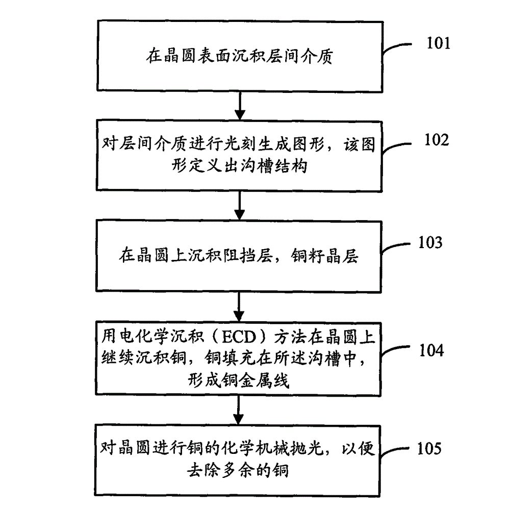
Method for constructing copper wire on wafer and chemical mechanical polishing (CMP) method for copper
A copper metal and wafer technology, which is applied in the field of semiconductor integrated circuit manufacturing, can solve the problems of depression at the metal wire, damage to the flatness of the wafer surface, and adverse effects of the conductive performance of the metal wire.
- Summary
- Abstract
- Description
- Claims
- Application Information
AI Technical Summary
Problems solved by technology
Method used
Image

Examples
Embodiment Construction
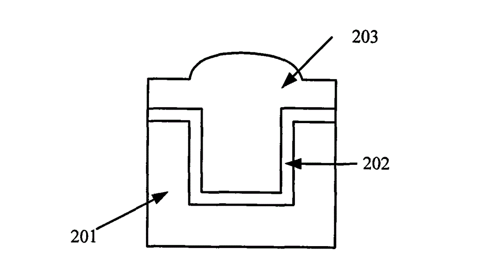
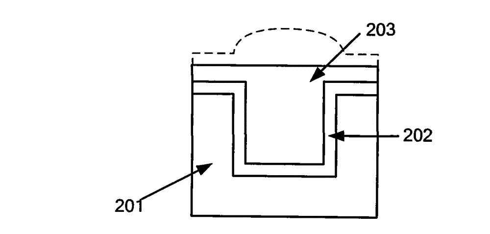
[0044] In the prior art, the main reason for causing the depression at the copper metal line is that the MRR difference between the interlayer dielectric and copper is relatively large. The key point of the method for constructing copper metal lines on a wafer proposed by the present invention is that after the first interlayer dielectric is deposited on the surface of the wafer, the second interlayer dielectric is additionally deposited, and the material constituting the second interlayer dielectric The hardness is smaller than that of the material constituting the first interlayer medium. When the Cu-CMP process is performed, the second interlayer dielectric is removed together with copper, and the MRR of the second interlayer dielectric is closer to the MRR of copper than the MRR of the original first interlayer dielectric, which can effectively reduce The degree of dishing at the copper metal line after CMP.
[0045] In order to make the purpose, technical solution and ad...
PUM
| Property | Measurement | Unit |
|---|---|---|
| thickness | aaaaa | aaaaa |
| Brinell hardness | aaaaa | aaaaa |
| elastic modulus | aaaaa | aaaaa |
Abstract
Description
Claims
Application Information