Eureka AIR delivers breakthrough ideas for toughest innovation challenges, trusted by R&D personnel around the world.

Method for improving width uniformity of grooves

A technology of groove width and uniformity, applied in the direction of electrical components, semiconductor/solid-state device manufacturing, circuits, etc., can solve the problems of poor groove width uniformity, poor feature size uniformity, etc., and improve the uniformity of groove width performance, improve uniformity, and increase the effect of groove width

Inactive Publication Date: 2013-01-16
SEMICON MFG INT (SHANGHAI) CORP +1
View PDF2 Cites 0 Cited by
  • Summary
  • Abstract
  • Description
  • Claims
  • Application Information

AI Technical Summary

Problems solved by technology

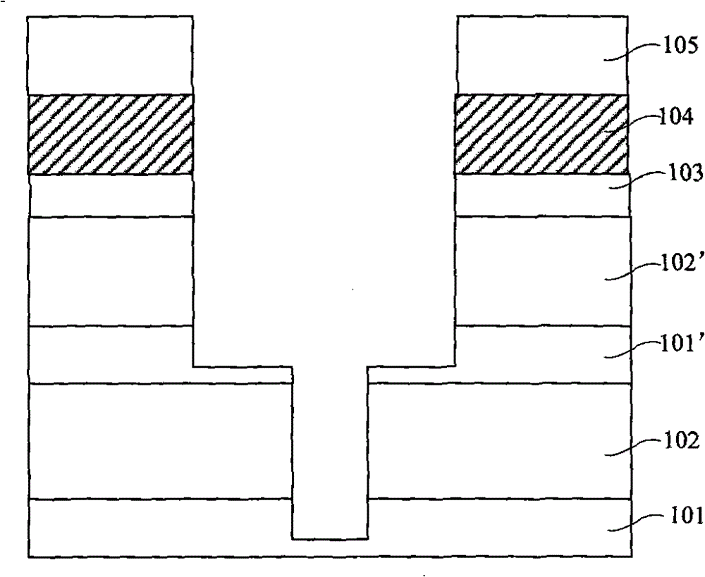
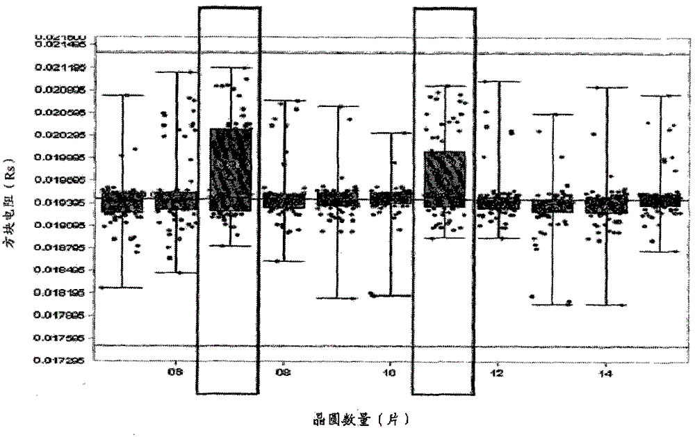
This shows that for the entire wafer, the uniformity of the trench width is poor, that is, the poor uniformity of the feature size detected after etching (After Etch InspectionCritical Dimension Uniformity, AEI CDU)

Method used


Image

  • Method for improving width uniformity of grooves
  • Method for improving width uniformity of grooves
  • Method for improving width uniformity of grooves

Examples


Embodiment Construction

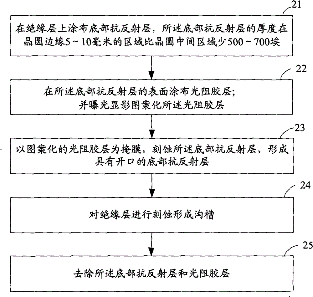
[0031] In the present invention, the insulating layer is etched to form a schematic flow chart of the method for trenching. figure 1 shown, including the following steps:

[0032] Step 21, coating the bottom anti-reflection layer on the insulating layer, that is, the hard mask layer in the specific embodiment. The bottom anti-reflection layer is necessary in this step, because the bottom anti-reflection layer not only acts as a light absorbing layer, but also acts as a blocking mask when etching the hard mask layer. Since the material of the bottom anti-reflective layer and the photoresist layer are the same, they are all organic materials, so when performing the following step 23, the photoresist layer is consumed at the same time, and when step 23 is completed, the photoresist layer is basically If it is consumed, it can no longer be used as a mask. Therefore, when etching the insulating layer and forming a trench, the bottom anti-reflection layer is used as a mask.

[00...


PUM


Abstract

The invention relates to a method for improving width uniformity of grooves, which comprises the steps of: coating a bottom anti-reflection layer on an insulation layer, wherein the thickness of the bottom anti-reflection layer on an area of 5-10mm of a wafer edge is 500-700 angstrom less than that on a wafer center area; coating a photo resistant adhesive layer on the surface of the bottom anti-reflection layer; exposing and developing to pattern the photo resistant adhesive layer; etching the bottom anti-reflection layer by taking the patterned photo resistant adhesive layer as a mask so asto form the bottom anti-reflection layer with an opening; and etching the insulation layer to form a groove and removing the bottom anti-reflection layer and the photo resistant adhesive layer. According to the method, the width uniformity of the etched groove can be effectively improved.

Description

technical field [0001] The invention relates to a semiconductor device manufacturing process, in particular to a method for improving the uniformity of the groove width. Background technique [0002] At present, in the back-end-of-line (BEOL) process of semiconductor devices, multiple layers of metal interconnection layers can be grown on semiconductor substrates according to different needs, and each layer of metal interconnection layers includes metal interconnection lines And the insulating layer, which requires the manufacture of trenches (trench) and connection holes for the above-mentioned insulating layer, and then deposit metal in the above-mentioned trenches and connection holes, the deposited metal is the metal interconnection line, and copper is generally selected as the metal interconnection wire material. The insulating layer can be specifically set according to the needs of the manufacturing process. For example, it includes an etching stop layer formed seque...

Claims


Application Information

Patent Timeline
Patent Type & Authority Patents(China)
IPC IPC(8): H01L21/768H01L21/311
Inventor 孙武
Owner SEMICON MFG INT (SHANGHAI) CORP
Why Eureka
Eureka Blog
Learn More