Unlock instant, AI-driven research and patent intelligence for your innovation.

Active element array substrate, display panel and repairing method

A technology of active components and array substrates, which is applied in the direction of electrical components, electric solid devices, semiconductor devices, etc., can solve the problems of incomplete curing of the frame glue, and achieve the effect of solving incomplete curing and reducing the resistance and capacitance load

Inactive Publication Date: 2012-08-08
AU OPTRONICS CORP
View PDF0 Cites 0 Cited by
  • Summary
  • Abstract
  • Description
  • Claims
  • Application Information

AI Technical Summary

Problems solved by technology

[0006] The present invention also provides a display panel, which can solve the problem of incomplete curing of the sealant caused by the metal grid in the drive circuit

Method used


Image

  • Active element array substrate, display panel and repairing method
  • Active element array substrate, display panel and repairing method
  • Active element array substrate, display panel and repairing method

Examples


Embodiment Construction

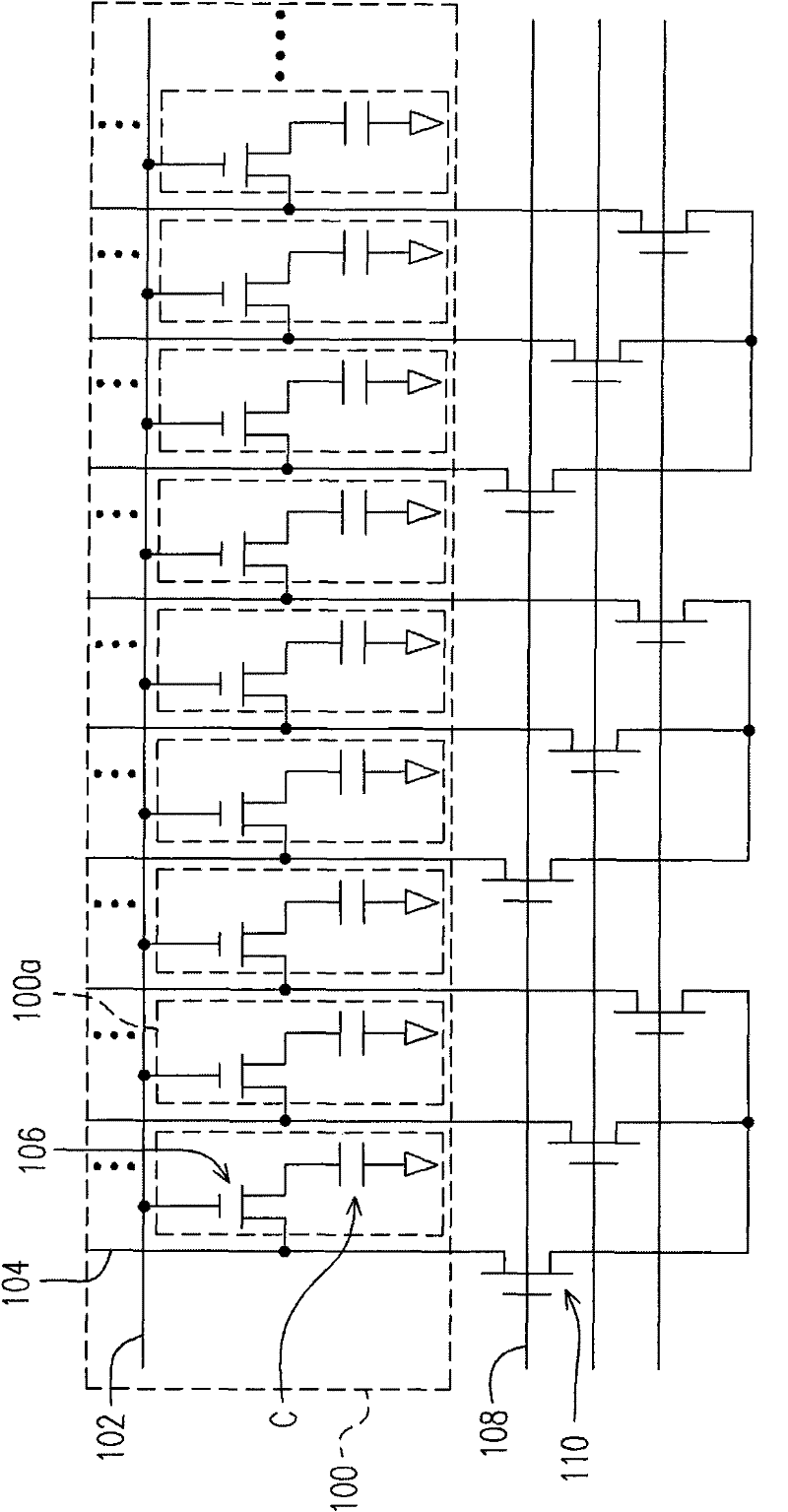
[0052] figure 1 It is a schematic circuit diagram of an active device array substrate according to an embodiment of the present invention. exist figure 1 In order to make the drawing clear and easy to explain, only one scan line is shown, but it should be understood that there are multiple scan lines in the active device array substrate. Please refer to figure 1 , the active element array substrate has a display area 100 . The active device array substrate includes a substrate (shown in figure 2 , which will be described later), the first signal line, the second signal line, the active element 106 , the pixel electrode (not shown), the bus 108 and the switching element 110 . In this embodiment, the first signal line is the scan line 102 , and the second signal line is the data line 104 .

[0053] The scan lines 102 and the data lines 104 are arranged alternately on the substrate to define a plurality of pixel areas 100 a in the display area 100 . The active devices 106 ...


PUM


Abstract

The invention relates to an active element array substrate, a display panel and a repairing method. The active element array substrate comprises a substrate, a first signal wire, a second signal wire, an active element, a pixel electrode, a bus and a switch element, wherein the bus and the switch element are allocated outside a display area of the active element array substrate; the switch element is provided with a grid, a first electrode and a second electrode; the grid is coupled with the bus; the first electrode and the second electrode are positioned on the upper side of the grid; the first electrode is coupled to a signal source; the second electrode is coupled to the first signal wire; the first electrode and the second electrode are in a comb shape respectively; the first electrode comprises a plurality of first finger parts parallel to one another and first connection parts connected with the first finger parts; the second electrode comprises a plurality of second finger parts parallel to one another and second connection parts connected with the second finger parts; the first finger parts and the second finger parts are alternatively arranged; and partial first electrodes are positioned outside the grid.

Description

technical field [0001] The present invention relates to an active element array substrate, a display panel and a repair method, and in particular to an active element that can reduce the resistance and capacitance load (RC loading) during signal transmission and solve the short circuit problem caused by metal particles. Element array substrate, display panel and repair method. Background technique [0002] In general displays, due to the high parasitic capacitance (C gd with C gs ), therefore, when a bottom-gate TFT is used as a transistor in a driving circuit, a relatively large resistance-capacitance load is often generated in signal transmission. [0003] In addition, generally speaking, the bottom gate thin film transistor in the driving circuit is usually arranged on the coating path of the sealant, so when the sealant is cured by ultraviolet light, the metal in the bottom gate thin film transistor The gate will cause incomplete curing of the sealant. [0004] In ad...

Claims


Application Information

Patent Timeline
Patent Type & Authority Patents(China)
IPC IPC(8): H01L27/02H01L29/417H01L23/52H01L21/77
Inventor 邱皓麟高逸群
Owner AU OPTRONICS CORP
Features
  • R&D
  • Intellectual Property
  • Life Sciences
  • Materials
  • Tech Scout
  • Unparalleled Data Quality
  • Higher Quality Content
  • 60% Fewer Hallucinations
Learn More