Fin-type tunneling transistor integrated circuit and manufacturing method thereof

A technology of tunneling transistors and integrated circuits, which is applied in the direction of transistors, semiconductor/solid-state device manufacturing, circuits, etc., can solve problems such as limiting device performance, achieve low power consumption, reduce chip power consumption, and increase drive current effects

Inactive Publication Date: 2011-02-09
FUDAN UNIV
View PDF6 Cites 27 Cited by
  • Summary
  • Abstract
  • Description
  • Claims
  • Application Information

AI Technical Summary

Problems solved by technology

[0004] Although the leakage current of the planar tunneling field effect transistor is lower than that of the traditional MOS transistor, which can greatly reduce the power consumption of the chip, its driving current is two or three orders of magnitude smaller than that of the MOS transistor, which limits the performance of the device. It is necessary to use a new type of device to obtain a larger drive current

Method used


Image

  • Fin-type tunneling transistor integrated circuit and manufacturing method thereof
  • Fin-type tunneling transistor integrated circuit and manufacturing method thereof
  • Fin-type tunneling transistor integrated circuit and manufacturing method thereof

Examples


Embodiment Construction

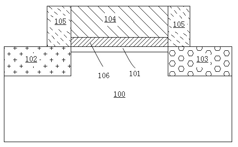
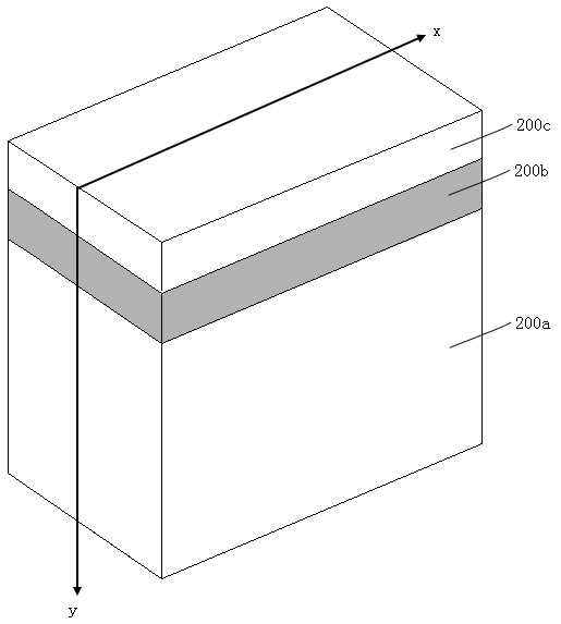
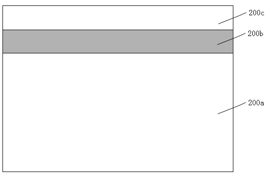
[0033] Exemplary embodiments of the present invention will be described in detail below with reference to the accompanying drawings. In the drawings, the thicknesses of layers and regions are exaggerated for convenience of illustration, and the shown sizes do not represent actual sizes. The referenced figures are schematic illustrations of idealized embodiments of the invention, and the illustrated embodiments of the invention should not be construed as limited to the particular shapes of regions illustrated in the figures but are to include resulting shapes, such as manufacturing-induced deviations. For example, the curves obtained by etching are usually curved or rounded, but in the embodiment of the present invention, they are all represented by rectangles. The representation in the figure is schematic, but this should not be considered as limiting the scope of the present invention. Meanwhile, in the following description, the term substrate used can be understood to inclu...


PUM


Abstract

The invention belongs to the technical field of manufacturing of semiconductor integrated circuits, and in particular relates to a fin-type tunneling transistor integrated circuit and a manufacturing method thereof. On the basis of a silicon-on-insulator substrate, a tunneling transistor has a fin-type grid structure, a high-k dielectric is used as a grid dielectric and a low-k dielectric is used as a side wall material. The drive current of the fin-type tunneling transistor integrated circuit is improved, the switching speed of the integrated circuit is increased and the power consumption of a chip is reduced. Further, the invention also discloses the method for manufacturing the fin-type tunneling transistor integrated circuit.

Description

technical field [0001] The invention belongs to the technical field of manufacturing semiconductor integrated circuits below 30 nanometers, specifically relates to a semiconductor integrated circuit and a manufacturing method thereof, in particular to a fin-type tunneling transistor (Fin-TFET) integrated circuit and a manufacturing method thereof. Background technique [0002] Metal-oxide-silicon field-effect transistors (MOSFETs) are widely used in various electronic products. With the development of integrated circuit technology, the size of MOSFET is getting smaller and smaller, and the density of transistors on the unit array is getting higher and higher. The ensuing short channel effect is also more obvious. How to reduce the power consumption of portable devices has become a research hotspot in the field of semiconductor technology. Today's integrated circuit device technology node is already at about 50 nanometers, and the leakage current between the source and drai...

Claims


Application Information

Patent Timeline
Patent Type & Authority Applications(China)
IPC IPC(8): H01L27/088H01L21/786H01L29/10
Inventor 臧松干刘昕彦王鹏飞张卫
Owner FUDAN UNIV
Why Eureka
Try Eureka