Charge pump circuit

A technology of charge pump and circuit, applied in the field of charge pump, which can solve problems such as burnout, increase of transistor switch SW3, time delay, etc.

Inactive Publication Date: 2011-02-09
GREEN SOLUTION TECH CO LTD
View PDF1 Cites 6 Cited by
  • Summary
  • Abstract
  • Description
  • Claims
  • Application Information

AI Technical Summary

Problems solved by technology

However, there is a time delay in the switching voltage conversion process, so during the conversion process, the transistor switches SW1, SW3 will be turned on at the same time, as Figure 2A As shown, the current Is will cause the transistor switches SW1 and SW3 to overheat and burn out
Also, please refer to Figure 2B , when the short-circuit state occurs in the second sequence, the transistor switches SW3 and SW4 are turned on, so

Method used


Image

  • Charge pump circuit
  • Charge pump circuit
  • Charge pump circuit

Examples


Embodiment Construction

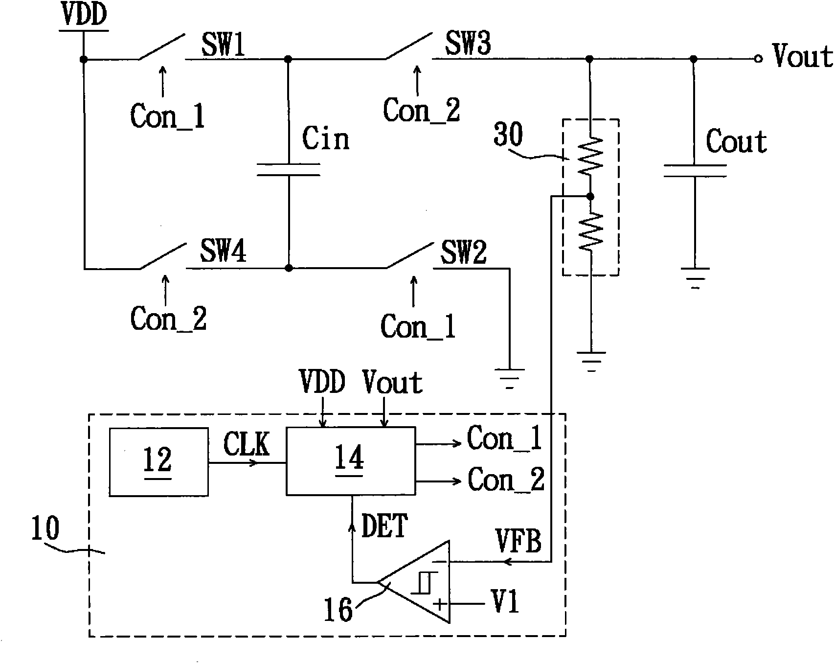
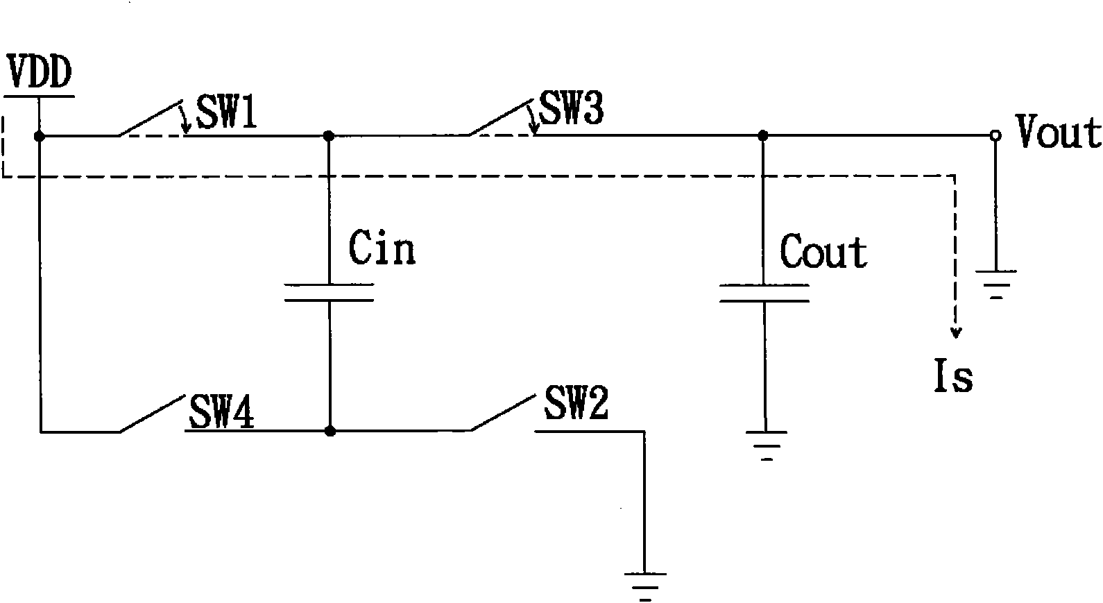
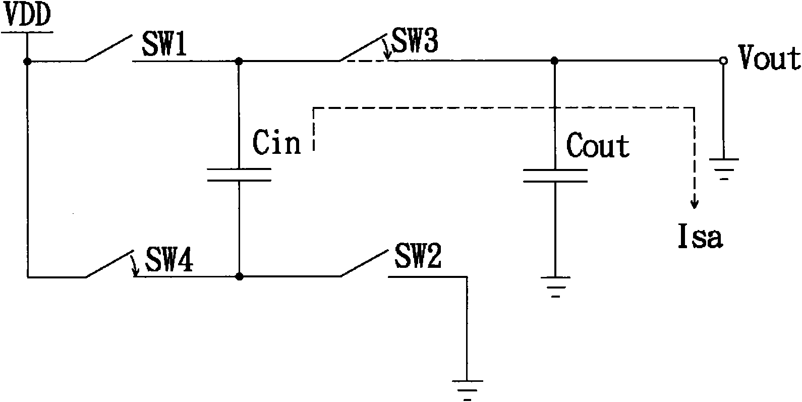
[0046] Please refer to image 3 , image 3 It is a schematic diagram of a charge pump circuit according to a first preferred embodiment of the present invention. The charge pump circuit includes a control unit 100 , a first capacitor unit Ci, a second capacitor unit Co, a charging path and a discharging path. The charging path includes a first P-type metal-oxide-semiconductor transistor PM1, a second N-type metal-oxide-semiconductor transistor NM2, and an input rectifying element D1. The first P-type MOS transistor PM1 is connected to an input voltage VDD and a first terminal of the first capacitor unit Ci, and the negative terminal of the parasitic diode is connected to the input voltage VDD, and the positive terminal is connected to the output voltage Vout. The second NMOS transistor NM2 is connected to a second terminal of the first capacitor Ci and the ground, and the negative terminal of the parasitic diode is connected to the input voltage VDD, and the positive termina...


PUM


Abstract

The invention discloses a charge pump circuit. The charge pump circuit is prevented from generating reverse flow by using a rectifier element, which can prevent energy stored in the charge pump circuit from reversely flowing into an input voltage source or energy stored in a capacitor at the output end from reversely flowing to the charge pump circuit and an input voltage source. A current limit unit is connected with an input power supply or/and connected to the output end, the invention can also avoid the problem that the input power supply provides heavy current to the charge pump circuit or/and the charge pump circuit provides heavy current to the output end to cause the overburning of elements of the charge pump circuit when generating short circuit.

Description

technical field [0001] The invention relates to a charge pump, in particular to a charge pump with reverse current prevention and current limiting. Background technique [0002] Please refer to figure 1 , figure 1 It is a schematic circuit diagram of an existing charge pump circuit. The charge pump circuit includes a full bridge switching circuit, a first capacitor Cin, a second capacitor Cout, a voltage feedback circuit 30 and a control element 10 . The full-bridge switching circuit includes four transistor switches SW1 - SW4 , which are controlled by the control signals Con_1 and Con_2 of the control element 10 . The control element 10 generates the control signal Con_1 at a first timing to control the conduction of the transistor switches SW1 and SW2 to form a first conduction path. At this time, the first capacitor Cin stores power transmitted by an input voltage VDD through the first conduction path. The control element 10 generates a control signal Con_2 at a seco...

Claims


Application Information

Patent Timeline
IPC IPC(8): H02M3/07
Inventor 徐献松柳娟娟
Owner GREEN SOLUTION TECH CO LTD
Why Eureka
Try Eureka