Method for physically implementing special integrated circuit chip under deep sub-micron

A deep submicron, integrated circuit technology, applied in the direction of electrical digital data processing, special data processing applications, instruments, etc., can solve the problems of timing convergence, inability to predict, transistor threshold voltage shrinkage, etc., and achieve good practical results Effect

Inactive Publication Date: 2011-03-16
杭州开鼎科技有限公司
View PDF2 Cites 18 Cited by
  • Summary
  • Abstract
  • Description
  • Claims
  • Application Information

AI Technical Summary

Problems solved by technology

[0002] At present, the integrated circuit manufacturing process has entered deep submicron, which brings new challenges to the physical realization of ASIC chips. The physical implementation process has a significant impact on timing convergence, and cannot be accurately estimated in the front-end logic design; second, as the feature size continues to shrink, the physical effects of various parasit...

Method used


Image

  • Method for physically implementing special integrated circuit chip under deep sub-micron
  • Method for physically implementing special integrated circuit chip under deep sub-micron
  • Method for physically implementing special integrated circuit chip under deep sub-micron

Examples


Embodiment Construction

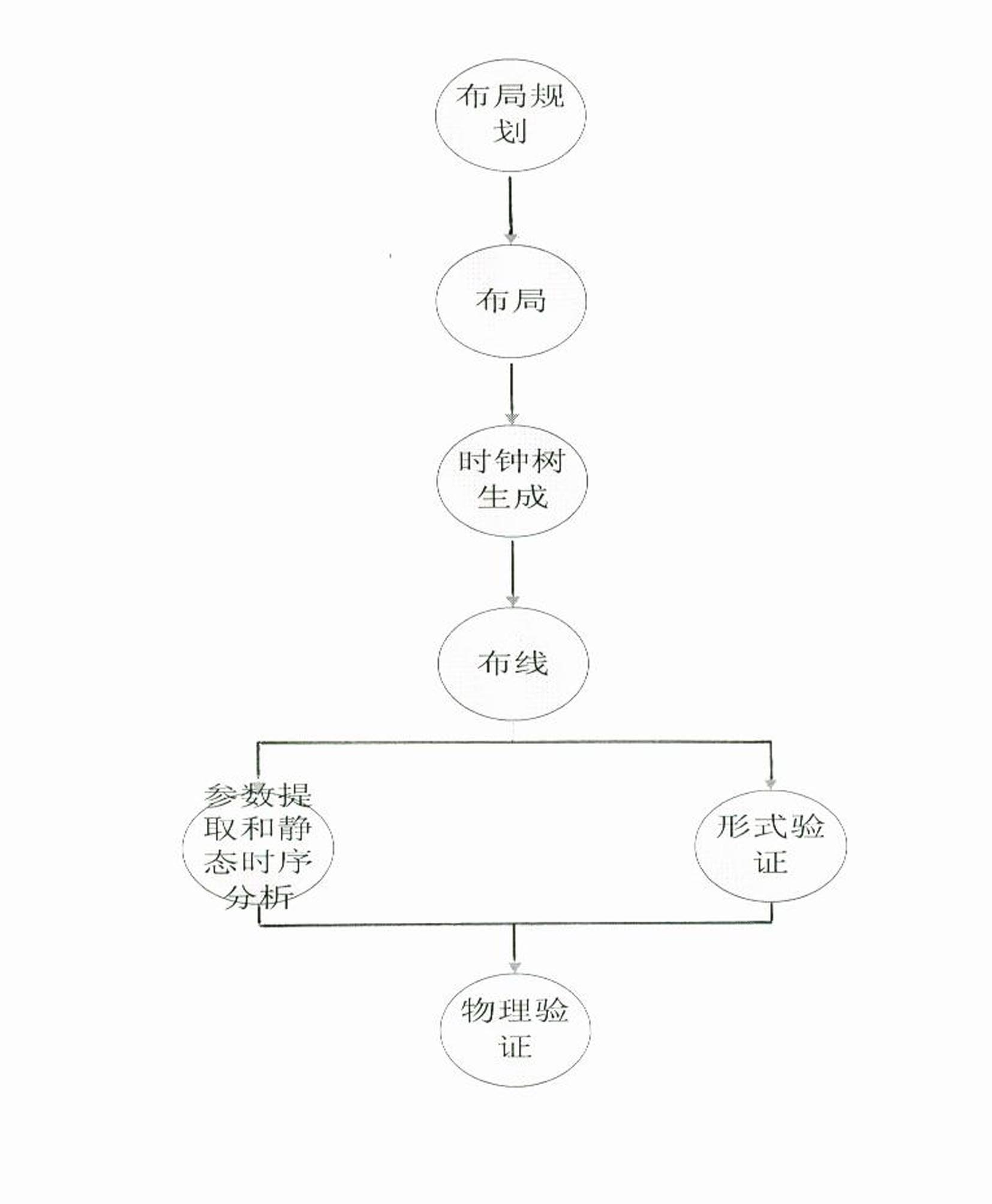
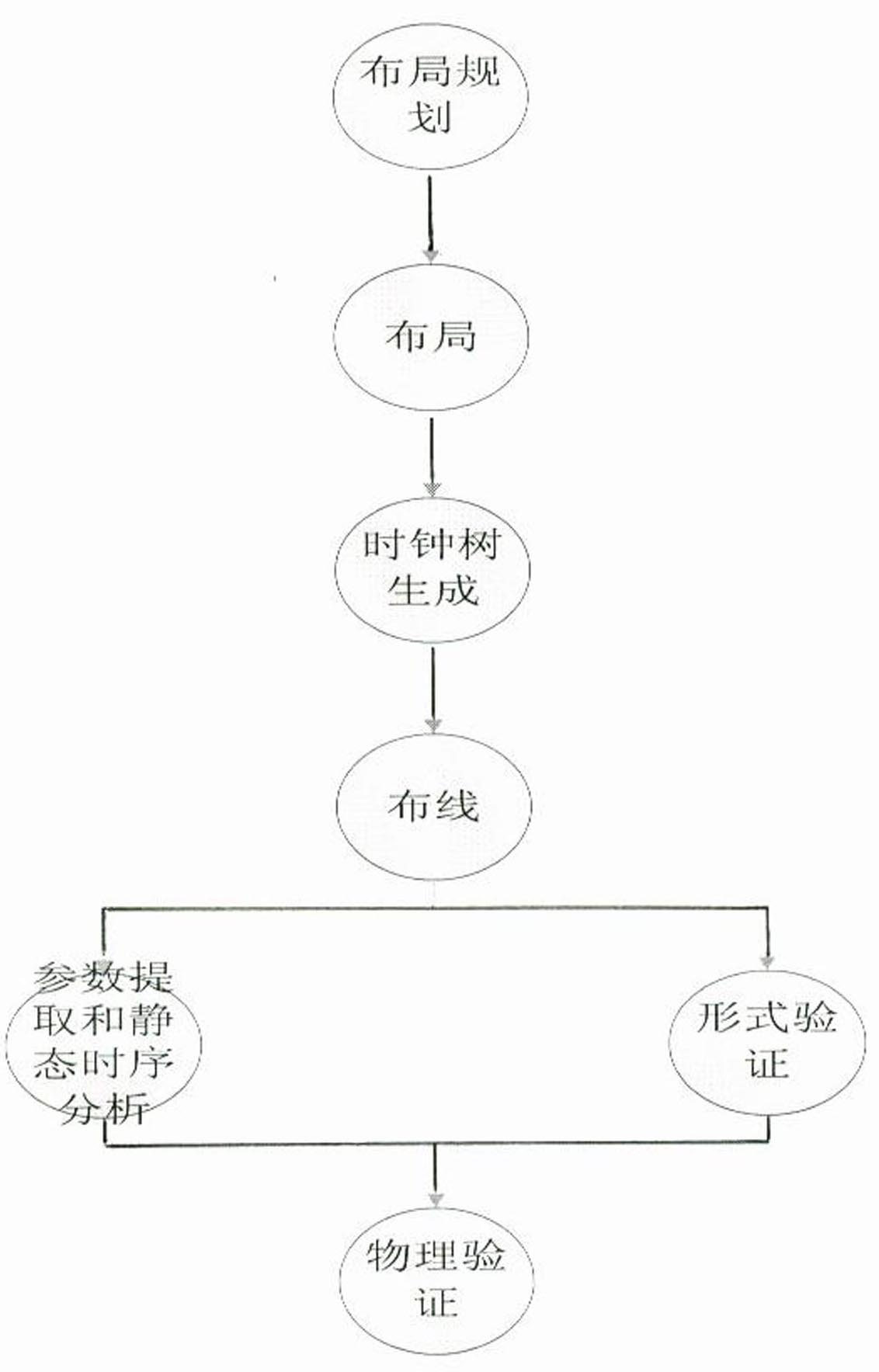
[0009] The present invention will be described in detail below in conjunction with accompanying drawing: figure 1 Shown: the physical realization method of the present invention comprises the following contents:

[0010] 1. Layout planning: Complete the determination of chip height and width, complete the arrangement of PAD, complete the placement of RAM, and complete power supply planning. The arrangement of the PAD also considers multiple factors such as the convenience of routing the chip to the PCB board in the future, the ease of implementation inside the chip, and SSO. Sensitive ports such as clocks use PADs with Schmitt hysteresis effects to improve noise immunity. The number of RAM units reaches 125, occupying 70% of the chip area. Combined with the reasonable planning of data flow, a certain space needs to be reserved between each RAM unit to place clock drive components. The electric-ground network adopts the combination of ring and stripe, and finally achieves...


PUM


Abstract

The invention provides a method for physically implementing a special integrated circuit chip under deep sub-micron. The method mainly comprises the following steps of: 1) planning layout; 2) laying out; 3) generating a clock tree; 4) wiring; and 5) extracting parameters and analyzing a static time sequence: extracting a parasitic parameter of the layout by adopting a parasitic parameter extraction tool, analyzing the static time sequence, and searching a key path according to the Breadth first search principle. The method has been applied to the practical chip developing process, passed practical tests, and has good practical using effect.

Description

technical field [0001] The invention relates to a physical realization method applied to a special integrated circuit chip in deep submicron, especially relates to a physical realization method under the condition of multiple storage units in the chip. Background technique [0002] At present, the integrated circuit manufacturing process has entered deep submicron, which brings new challenges to the physical realization of ASIC chips. The physical implementation process has a significant impact on timing convergence, and cannot be accurately estimated in the front-end logic design; second, as the feature size continues to shrink, the physical effects of various parasitic parameters have an impact on the correctness and reliability of the design , such as coupling, crosstalk, signal integrity, robustness of electrical and ground networks, etc.; third, the threshold voltage of transistors cannot be scaled down proportionally, the impact of subthreshold current is significant, ...

Claims


Application Information

Patent Timeline
IPC IPC(8): G06F17/50
Inventor 胡塘
Owner 杭州开鼎科技有限公司
Why Eureka
Try Eureka