Capacitor manufacturing method

A manufacturing method and capacitor technology, which is applied in semiconductor/solid-state device manufacturing, circuits, electrical components, etc., and can solve problems such as capacitor breakdown and difficult dielectric layer coverage

Inactive Publication Date: 2011-03-23
SEMICON MFG INT (SHANGHAI) CORP
View PDF0 Cites 5 Cited by
  • Summary
  • Abstract
  • Description
  • Claims
  • Application Information

AI Technical Summary

Problems solved by technology

[0010] The problem solved by the present invention is that in the existing capacitor manufacturing process, in the cross-sectional area of ​​the first insulating layer and the second insulating layer, the distance between the hemispheri...

Method used


Image

  • Capacitor manufacturing method
  • Capacitor manufacturing method
  • Capacitor manufacturing method

Examples


Embodiment Construction

[0028] The specific embodiments of the present invention will be described in detail below in conjunction with the accompanying drawings.

[0029] In order to solve the gap between two adjacent polysilicon hemispherical particles formed in the interface region of the first insulating layer and the second insulating layer in the prior art is too small, it is difficult to completely fill the dielectric layer material between the two hemispherical particles , the defect that the capacitor is easily broken down at the position, the present invention provides a new method for manufacturing a capacitor, and each step will be described in detail below in conjunction with the accompanying drawings. The method for manufacturing a capacitor includes:

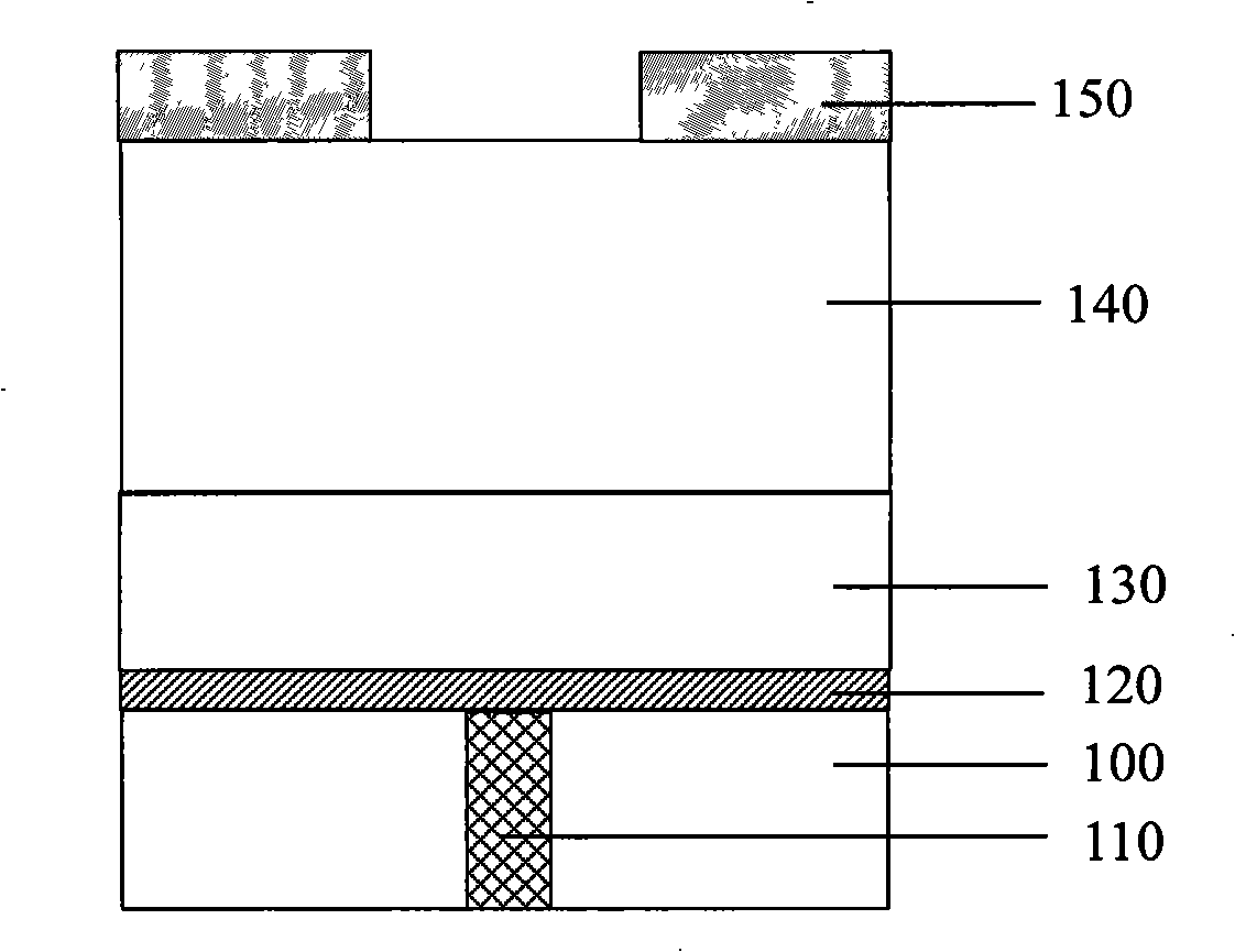
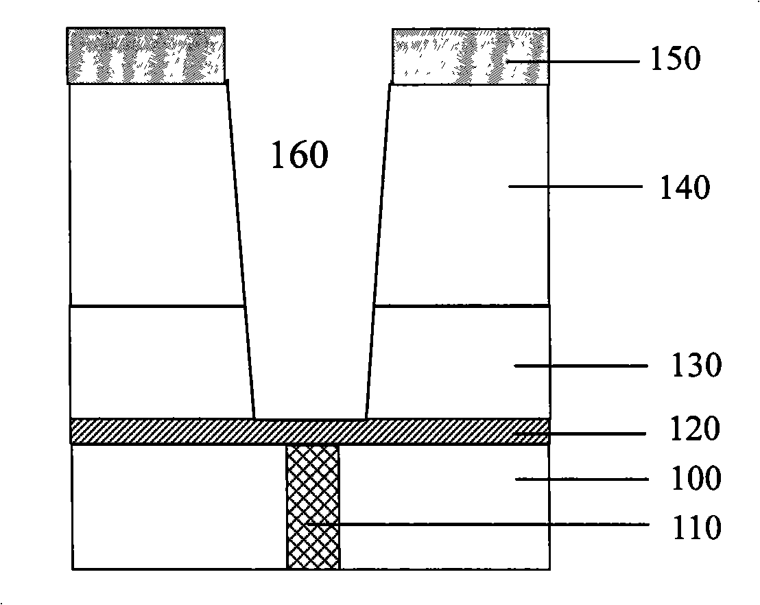
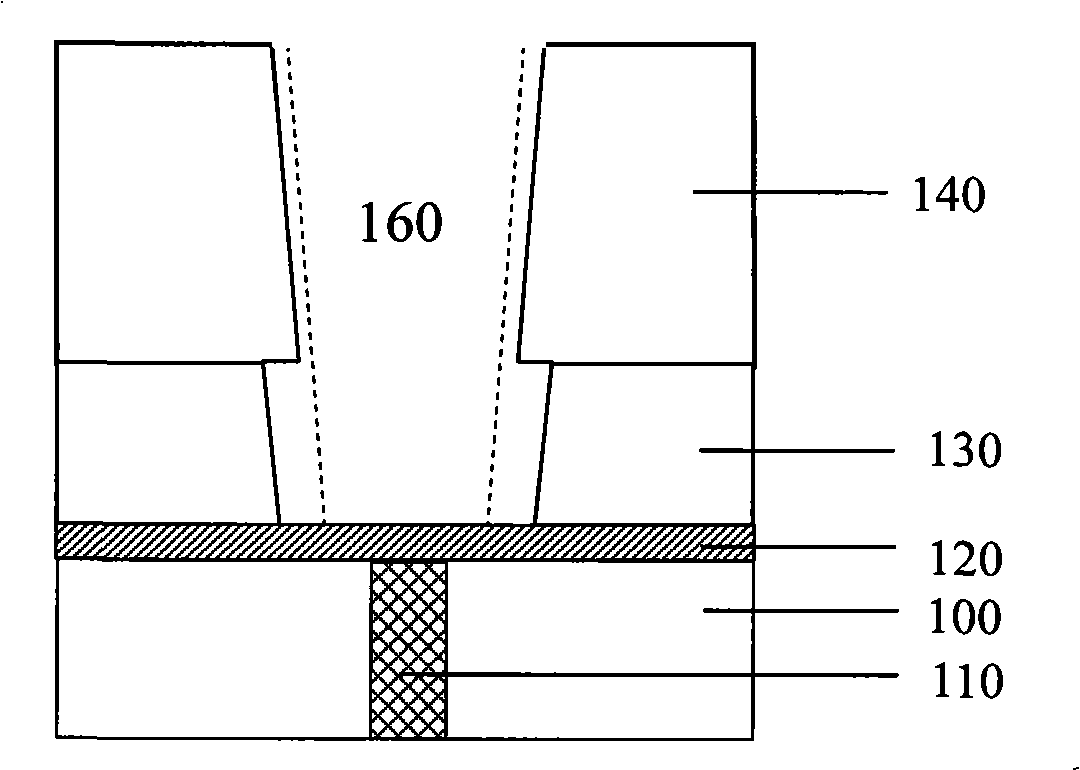
[0030] Step S1: providing an interlayer dielectric layer and an interconnection structure passing through the interlayer dielectric layer;

[0031] Reference attached Figure 3A As shown, 300 in the drawings is an interlayer dielectric l...


PUM


Abstract

The invention discloses a capacitor manufacturing method, which comprises the following steps: providing an inter-layer medium layer and an interconnection structure penetrating through the inter-layer medium layer; depositing an etching barrier layer, a first insulating layer, buffer layers and a second insulating layer on the inter-layer medium layer in turn; etching the second insulating layer, the buffer layer and the first insulating layer in turn to form grooves; etching the buffer layers through the grooves so as to increase the local widths of the grooves in the buffer layers; etching the grooves with a first etching agent, so that the bottom widths of the grooves approach to the top widths of the grooves; continuing to etch the grooves with a second etching agent, smoothening the closed angles at the interfaces between the second insulating layer and the buffer layers and between the buffer layers and the first insulating layer, and increasing the groove widths; removing the etching carrier layer; depositing polycrystalline silicon on the inner walls of the grooves and forming semi-spherical polycrystalline silicon particles serving as the lower electrode of the capacitor; and depositing a dielectric layer and an upper electrode on the lower electrode in turn. By using the method, the short circuit and the filling defect between the upper electrode and the lower electrode of the capacitor can be avoided.

Description

technical field [0001] The invention relates to the field of semiconductor manufacturing, in particular to a capacitor manufacturing method. Background technique [0002] As the critical dimension of semiconductor devices enters the sub-100nm era, the capacitance and reliability of capacitors play an increasingly important role for traditional single-transistor single-capacitor (1T-1C) structures. There are usually two ways to increase the capacitance of a capacitor. One is to increase the relative area between the upper and lower plates of the capacitor, and the other is to reduce the distance between the upper and lower plates of the capacitor. At present, in the semiconductor manufacturing process, more methods of increasing the relative area between the upper and lower plates of the capacitor are used to increase the capacitance. [0003] For the manufacturing method of capacitors in the existing 1T-1C structure, please refer to the attached Figure 1A to attach Figur...

Claims


Application Information

Patent Timeline
IPC IPC(8): H01L21/02H01L21/314
Inventor 罗飞邹立
Owner SEMICON MFG INT (SHANGHAI) CORP
Why Eureka
Try Eureka