Production method of optical element and optical element

一种光学元件、制造方法的技术,应用在光学元件、光学头制造、用光学方法记录/重现等方向,能够解决易发生剥离或裂纹、劣化、得不到树脂密合性等问题,达到抑制光学特性的变化、抑制吸收的效果

Inactive Publication Date: 2015-02-25
KONICA MINOLTA OPTO
View PDF8 Cites 0 Cited by
  • Summary
  • Abstract
  • Description
  • Claims
  • Application Information

AI Technical Summary

Problems solved by technology

[0004] However, when an antireflection film is formed on an optical element made of resin, since the film (mainly a metal oxide film) is generally an inorganic substance, compared with the case where glass is used as a base material, there are problems with the use of the base material. The difference in the coefficient of linear expansion of the resin becomes large, and problems such as peeling or cracking (cracks) tend to occur
In particular, SiO, which is generally used as an anti-oxidation film or hard coat 2 When used as the first layer, there is a problem that sufficient adhesion to the resin cannot be obtained
However, considering the necessity of necessary optical characteristics, the materials that are not desirable to be used are limited, and a solution is desired.
In addition, when a laser with a wavelength of 380 to 420 nm is used as a light source, the degradation of the resin substrate itself due to the energy of the laser itself and the further increase in the density of the recording medium inevitably require improvement in optical precision, and changes in optical properties due to moisture absorption of the resin are also inevitable. become a problem

Method used


Image

  • Production method of optical element and optical element
  • Production method of optical element and optical element
  • Production method of optical element and optical element

Examples


Embodiment

[0294] (1) Production of samples

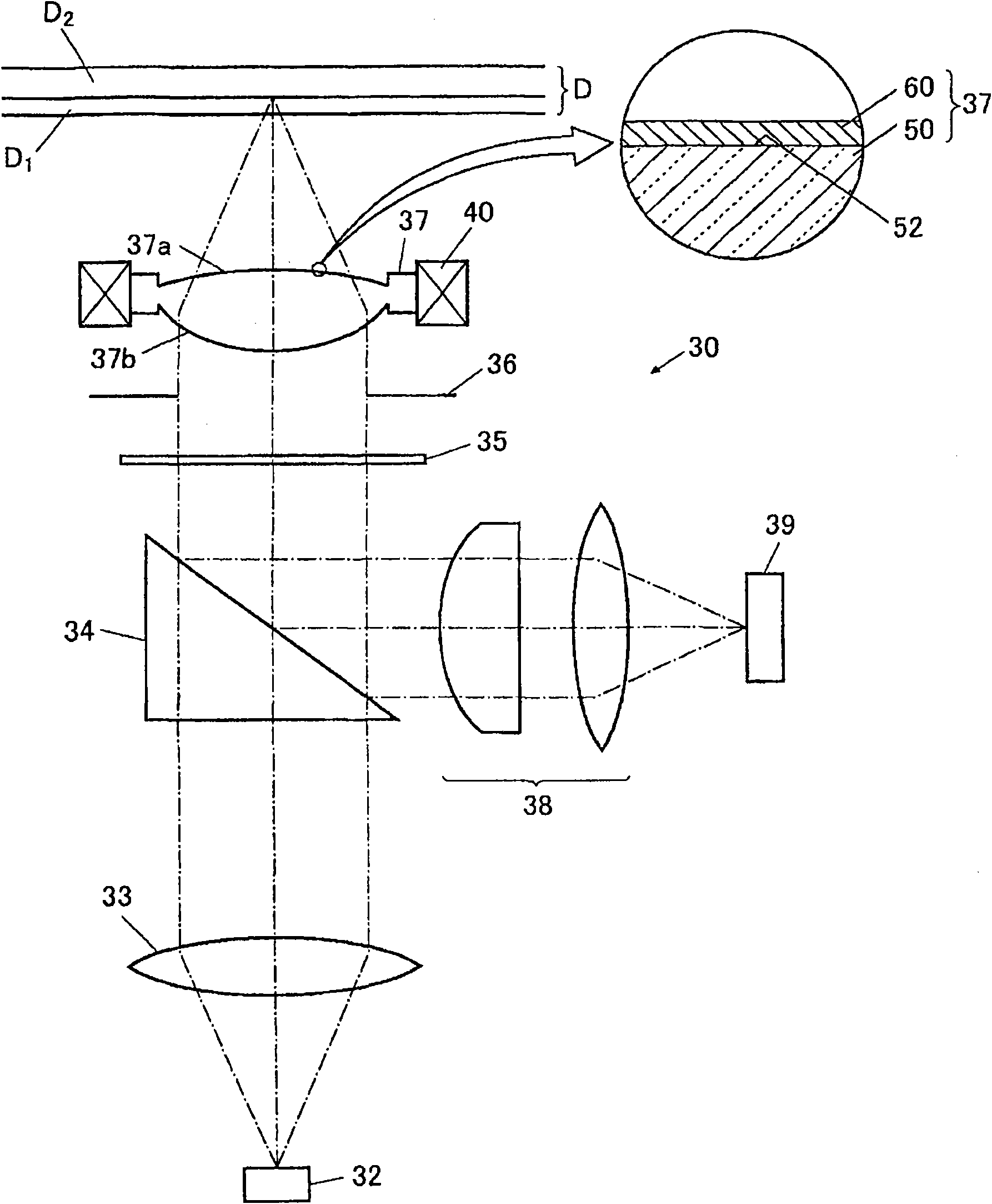
[0295] As the resin, ZEONEX-350R manufactured by Nippon Zenon Co., Ltd. was used, and the resin was injection-molded to form a resin molded part (resin lens).

[0296] As a resin lens, an objective lens of an optical pickup device dedicated to blue lasers having an effective diameter of 1 mm and an axial thickness of 1.57 mm was formed.

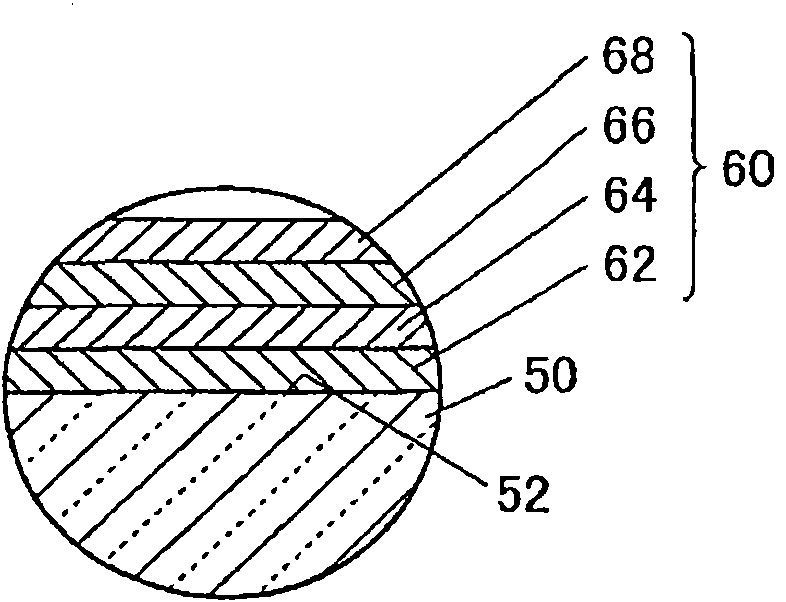
[0297] Then, for the resin molded part, the layers described in Table 1 and Table 2 were formed and laminated by vacuum vapor deposition using an electron beam. In this film-forming process, the O 2 The gas introduction pressure and the layer thickness of each layer were set as shown in Table 1 and Table 2.

[0298] Then, oxidation treatment is performed on the resin molded part on which the multilayer film was formed.

[0299] As an oxidation treatment, it was preserved for 48 hours in an environment of 60° C. and 80% RH.

[0300] According to the film composition (film thickness, O 2 Gas introduction ...


PUM

PropertyMeasurementUnit
wavelengthaaaaaaaaaa
coating thicknessaaaaaaaaaa

Abstract

A production method of an optical element, which is utilized in a pickup apparatus using a light source emitting light having wavelength of 380 nm to 420 nm and has a functional layer such as an anti-reflection film 60 formed on a molded portion 50 comprising a resin having an alicyclic structure, comprising steps of forming a first SiO layer 62 in the molded portion 50 by a vapor deposition process using SiO as an evaporation source and introducing O2 gas under a predetermined pressure, forming a second SiO layer 64 on the first SiO layer by a vapor deposition process using SiO as an evaporation source and introducing O2 gas under a pressure lower than the pressure used in forming the first SiO layer 62, and oxidizing the first SiO layer 62 and the second SiO layer 64.

Description

technical field [0001] The invention relates to a manufacturing method of an optical element and the optical element. Background technique [0002] In recent years, in optical devices such as optical pickup devices, compared with conventional CDs using a light source with a wavelength of about 780nm and DVDs using a light source with a wavelength of about 650nm, in order to further increase the recording density and increase the recording capacity, a An optical device corresponding to a Blu-ray Disc (hereinafter sometimes referred to as "BD") using laser light with a wavelength of 380 to 420 nm. [0003] On the other hand, optical elements such as objective lenses and collimator lenses used in such optical devices are expected to be manufactured with resins that can be manufactured easily and at low cost compared with glass with high manufacturing costs. High light transmittance, often forming anti-reflection film. [0004] However, when an antireflection film is formed on...

Claims


Application Information

Patent Timeline
Patent Type & Authority Patents(China)
IPC IPC(8): G02B1/11G11B7/22G02B1/10G02B1/115G02B3/00
CPCG11B7/1374G02B1/113
Inventor 粕谷仁一
Owner KONICA MINOLTA OPTO
Why Eureka
Try Eureka