
Display device and driving method thereof

A technology of a display device and a driving method, applied to static indicators, instruments, etc., can solve the problems of manufacturing process characteristic deviation, inter-pixel brightness deviation, driving current deviation, etc. Effects of Correcting Variation in Writing Characteristics

Inactive Publication Date: 2011-03-30
HITACHI DISPLAYS +1
View PDF5 Cites 4 Cited by
  • Summary
  • Abstract
  • Description
  • Claims
  • Application Information

AI Technical Summary

Problems solved by technology

[0003] On the other hand, such a driving transistor for controlling the amount of current flowing to a self-luminous element has variations in characteristics due to unevenness in its manufacturing process
This characteristic variation leads to variation in the drive current from the light-emitting element, and eventually causes luminance variation between pixels, which becomes a cause of image quality degradation

Method used


Image

  • Display device and driving method thereof
  • Display device and driving method thereof
  • Display device and driving method thereof

Examples


Embodiment approach 1

[0032]

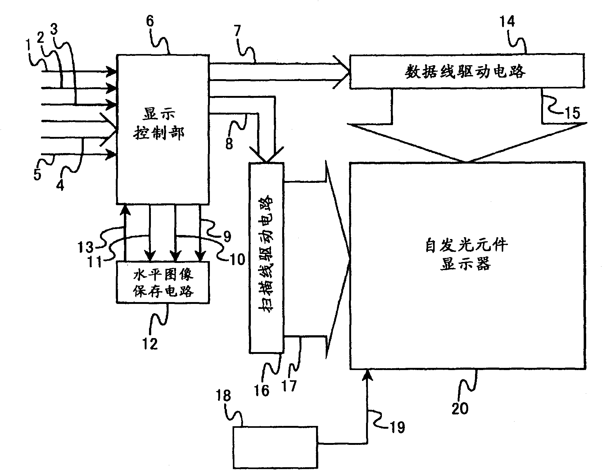
[0033] figure 1 It is a diagram for explaining the schematic configuration of the display device according to the first embodiment of the present invention, particularly a configuration diagram of an embodiment of an image display device using a self-luminous element. in figure 1 In the figure, vertical synchronization signal 1, horizontal synchronization signal 2, data enable 3, display data 4, synchronization clock 5, display control unit 6, data line control signal 7, scan line control signal 8, storage circuit control signal 9 , Save circuit control address 10, save data 11, horizontal image save circuit 12, read data 13, data line drive circuit 14, data line drive signal 15, scan line drive circuit 16, scan line drive signal 17, light-emitting voltage generation circuit 18. Self-luminous element light-emitting voltage 19 and self-luminous element display 20.

[0034] Vertical synchronization signal 1 is a signal of 1 cycle (1 frame period) of the display screen, hor...

Embodiment approach 2

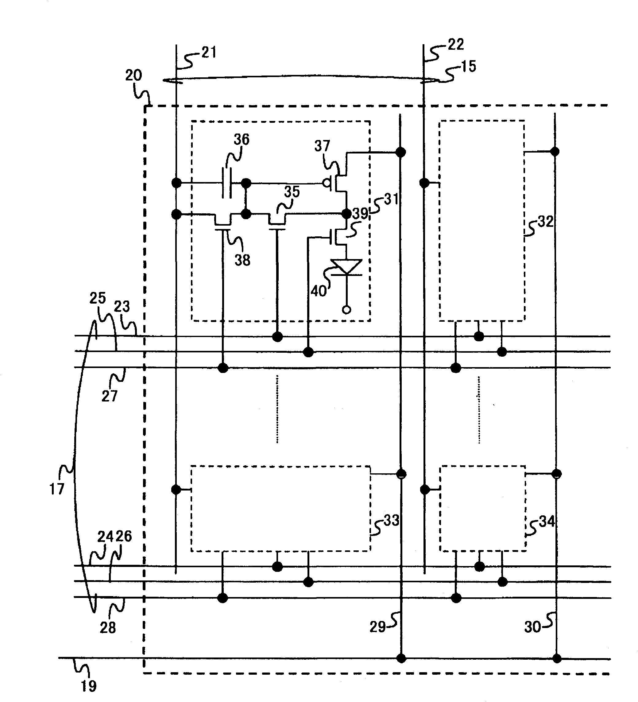
[0098] Figure 14 It is a waveform chart explaining the operation of the data drive circuit in the display device of the second embodiment of the present invention. Figure 15 It is a circuit diagram for explaining the internal structure of a pixel in the display device of Embodiment 2 of the present invention. Figure 14 The waveform group (a) of is a signal waveform related to an operation to be output for writing display data of one horizontal period to a pixel, and the waveform group (b) is a waveform in one frame period. In particular, in the waveform group (a), the time axis is enlarged compared to the waveform group (b), and a signal waveform that cannot be represented by the time scale of the waveform group (b) is displayed. In this embodiment, a correction switch is not provided and the control terminal of the drive inverter is set to a correction voltage via a write capacitor, which is different from the display device of the first embodiment. Except for these points, ...


PUM


Abstract

The invention provides a display device and a driving method thereof. The display device is capable of improving display quality by lightening the deviation of the driving current of a self-luminous element caused by the condition difference of the written data after the illumination and the characteristic change of driving transistor in a display device having pixels arrayed in matrix having the self-luminous element and the driving transistor. A data line drive circuit outputs a display signal voltage to data lines in a first period. Each pixel holds the display signal voltage with reference to a voltage determined based on characteristics of the driving transistor. In a second period, a control voltage for controlling the driving transistor is output to the data lines. The driving transistor generates a driving current in accordance with the control voltage and the held signal voltage so as to allow the self-luminous element to emit light. After the second period, a third period is arranged in which a voltage signal for setting a control terminal of the driving transistor to have a given correction voltage is output to the data lines. The first period follows the third period.

Description

Technical field [0001] The present invention relates to a display device and a driving method thereof, and more particularly to a self-luminous display device equipped with an EL (electroluminescence) element, an organic EL element, and other self-luminous type display elements, that is, a self-luminous element, and a driving method thereof. Background technique [0002] Among the self-luminous elements represented by EL elements, organic EL elements, etc., the light-emitting brightness is proportional to the amount of current flowing through the self-luminous element. This can be achieved by controlling the amount of current flowing through the self-luminous element. Grayscale display. A plurality of such self-luminous elements can be arranged to produce a display device. [0003] On the other hand, such drive transistors for controlling the amount of current flowing to the self-luminous element have variations in characteristics due to unevenness in the manufacturing process. T...

Claims


Application Information

Patent Timeline
Patent Type & Authority Applications(China)
IPC IPC(8): G09G3/32
CPCG09G2310/066G09G2320/043G09G2300/0861G09G2300/0842G09G3/3291G09G2310/0205G09G3/3258G09G2300/0819
Inventor 笠井成彦石井雅人河野亨秋元肇
Owner HITACHI DISPLAYS
Learn More