Method for manufacturing aluminum pad

A production method and technology of aluminum pads, which are applied in semiconductor/solid-state device manufacturing, electrical components, circuits, etc., can solve the problems of medium layer doping, product defects, and residues that cannot be cleaned thoroughly, so as to ensure quality and ensure product quality The effect of yield

Active Publication Date: 2013-01-30
SEMICON MFG INT (SHANGHAI) CORP
View PDF0 Cites 0 Cited by
  • Summary
  • Abstract
  • Description
  • Claims
  • Application Information

AI Technical Summary

Problems solved by technology

[0005] The technical problem to be solved by the present invention is to overcome the disadvantages in the prior art that when argon is used for physical pre-cleaning, the medium layer is easily mixed with metal impurities and residues cannot be cleaned thoroughly, which will cause product defects, and an improved aluminum pad is proposed Craftsmanship

Method used


Image

  • Method for manufacturing aluminum pad
  • Method for manufacturing aluminum pad
  • Method for manufacturing aluminum pad

Examples


Embodiment Construction

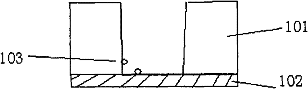
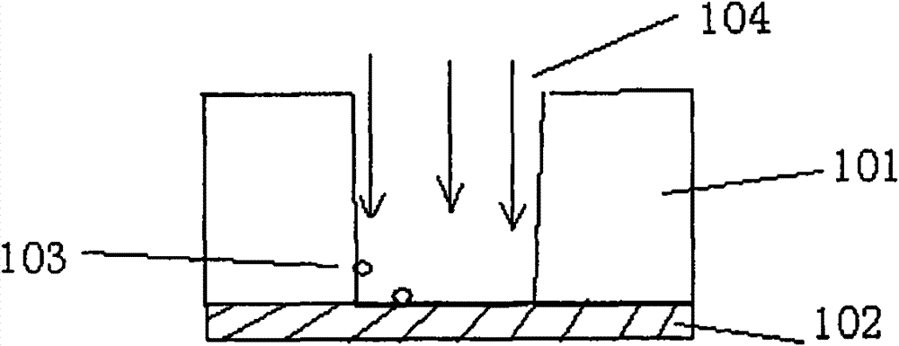
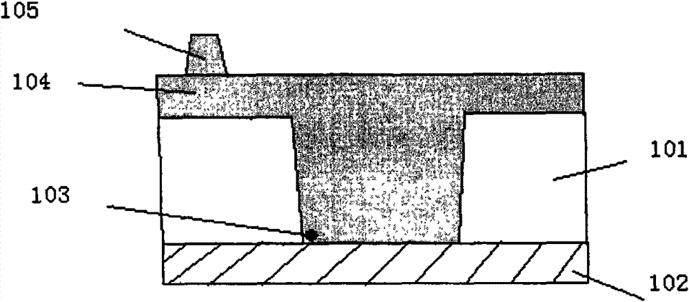
[0015] The embodiment of the present invention is by using nitrogen trifluoride (NF 3 ) and ammonia (NH 3 ) chemical cleaning method to pre-clean the aluminum pad base, thoroughly clean the residue on the aluminum pad base of the wafer, and avoid aluminum whiskers and gas leakage during the aluminum deposition process to ensure the conduction between the aluminum pad and the base completeness of the signal.

[0016] In order to make the above objects, features and advantages of the present invention more comprehensible, specific implementations of the present invention will be described in detail below in conjunction with the accompanying drawings.

[0017] figure 2 The production flowchart of the present invention includes the following steps: S200, at first providing the wafer with the aluminum pad base and the dielectric layer formed, etching the dielectric layer to expose the aluminum pad base to form a groove for depositing the aluminum pad; S201, using chemical The c...


PUM

PropertyMeasurementUnit
thicknessaaaaaaaaaa

Abstract

The invention relates to a method for manufacturing an aluminum pad, which comprises the following steps of: providing a wafer on which an aluminum pad substrate and a dielectric layer are formed, etching the dielectric layer to expose the aluminum pad substrate and form a groove for depositing the aluminum pad; pre-cleaning the aluminum pad substrate at the bottom of the groove and the dielectric layer on the side wall of the groove in a chemical cleaning mode; depositing a barrier layer; and depositing aluminum in the groove. The aluminum pad substrate and the side wall are cleaned from the upper parts in the chemical cleaning mode, so that residues and water-containing impurities cannot be left on the aluminum pad substrate and the dielectric layer, and the signal transmission quality of the aluminum pad in the subsequent process and the yield of products are guaranteed.

Description

technical field [0001] The invention relates to the field of semiconductors, in particular to a method for manufacturing an aluminum pad. Background technique [0002] In the field of integrated circuit manufacturing, logic products need to make aluminum gaskets, which are used as the test terminals connected by probe cards and the welding points of chip package pins during back-end testing, so aluminum pads are important for signal transmission and use during product testing. plays a very important role. [0003] Existing aluminum pad manufacturing process, refer to Figure 1A , first provide a semiconductor substrate, the semiconductor substrate is formed with an aluminum pad base 102, a dielectric layer 101 is formed on the aluminum pad base 102, the aluminum pad base 102 can be a copper interconnection layer, and the dielectric layer 101 can be silicon oxide , etch the dielectric layer 101 to expose the aluminum pad base 102 to form a groove for depositing the aluminum ...

Claims


Application Information

Patent Timeline
Patent Type & Authority Patents(China)
IPC IPC(8): H01L21/60H01L21/00
Inventor 何伟业聂佳相刘盛杨瑞鹏
Owner SEMICON MFG INT (SHANGHAI) CORP
Why Eureka
Try Eureka