Photoelectric conversion device and imaging system using the same

A technology of photoelectric conversion device and photoelectric conversion element, which is applied in parts of TV system, radiation control device, color TV parts, etc., can solve problems such as block breakdown, and achieve the effect of improving transmission efficiency

Active Publication Date: 2013-05-08
CANON KK
View PDF2 Cites 0 Cited by
  • Summary
  • Abstract
  • Description
  • Claims
  • Application Information

AI Technical Summary

Problems solved by technology

[0004] However, according to the configuration disclosed in Japanese Patent Application Laid-Open No. 2004-063498, since the photodiode is formed deep below the first gate electrode and the positions of the photodiode and the drain region are close to each other when the size of the pixel is reduced, Therefore, a breakdown may occur in the bulk, resulting in a conductive state

Method used


Image

  • Photoelectric conversion device and imaging system using the same
  • Photoelectric conversion device and imaging system using the same
  • Photoelectric conversion device and imaging system using the same

Examples


no. 1 example

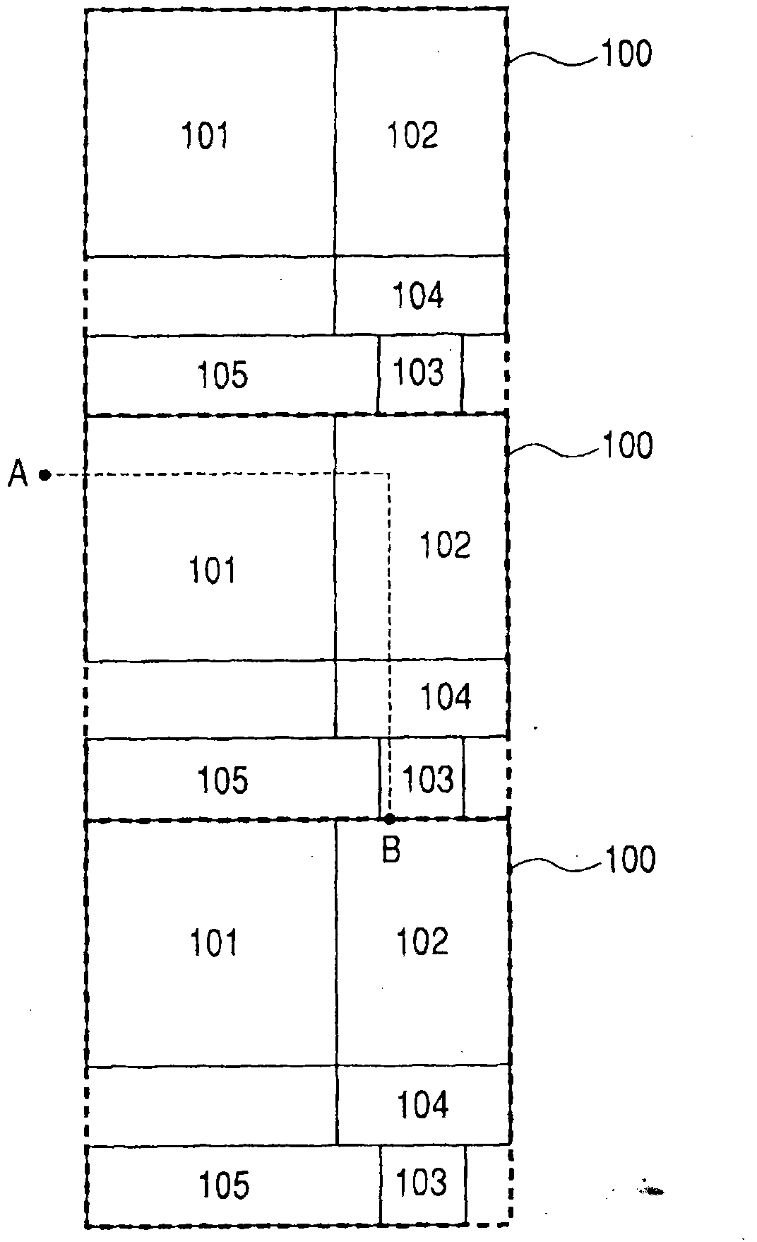
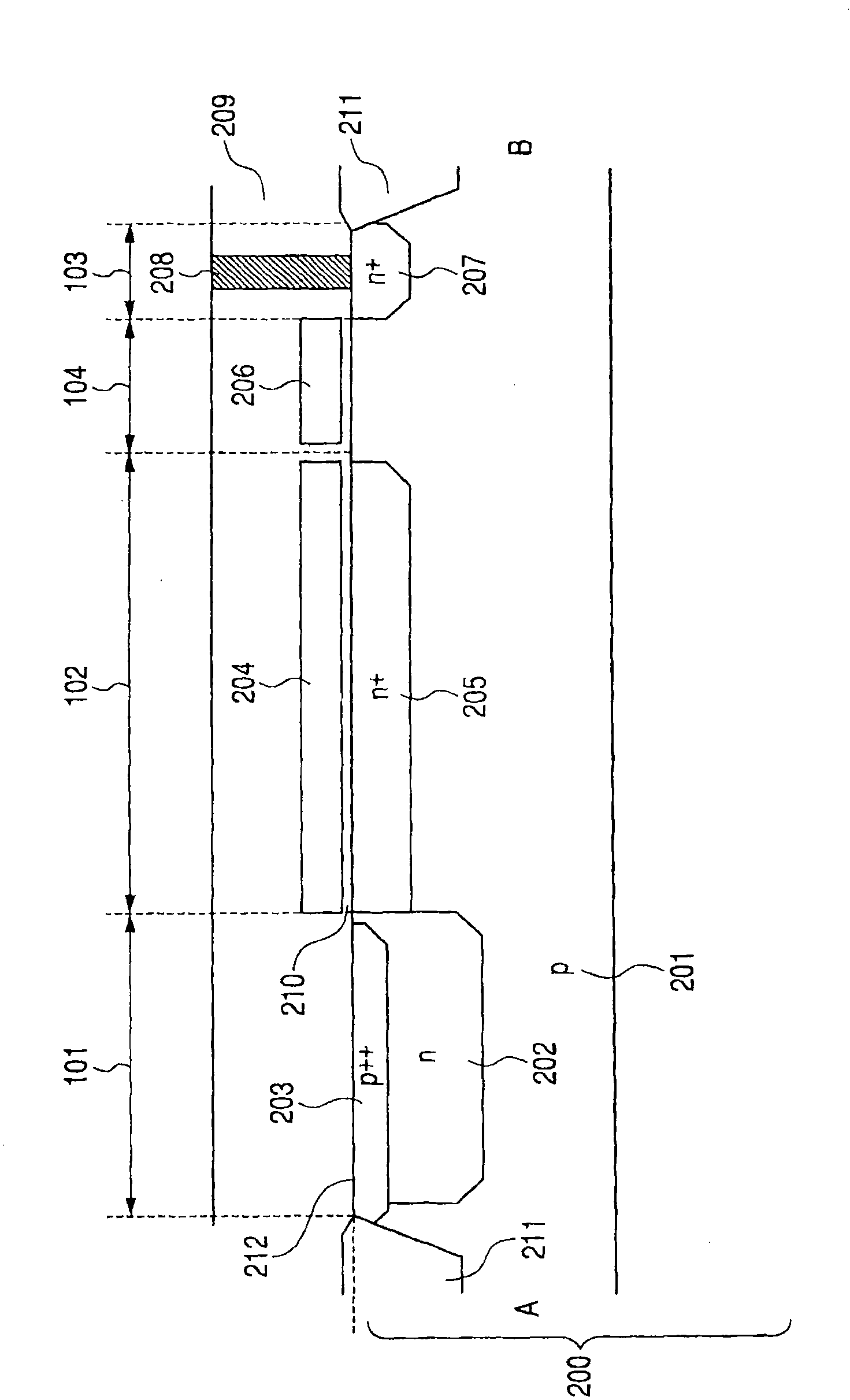
[0027] First, by using figure 1 A pixel to which the present invention is applicable is described. figure 1 is a schematic plan view showing elements as blocks. The pixel 100 includes a photoelectric conversion element 101, a charge storage portion 102, a floating diffusion region 103, and a charge transfer portion 104. The other elements are simply indicated collectively by reference numeral 105 . Other elements include, for example, MOS transistors for amplification and MOS transistors for reset, and may have any detailed configuration. Also, an element isolation region is omitted. A pixel is a minimum repeating unit having at least one photoelectric conversion element, and the pixels 100 are arranged one-dimensionally or two-dimensionally to form an imaging area. figure 1 An array of three pixels 100 is shown. figure 2 A cross-sectional view of such a pixel 100 taken along line A-B is shown.

[0028] figure 2 is along figure 1 A schematic cross-sectional view take...

no. 2 example

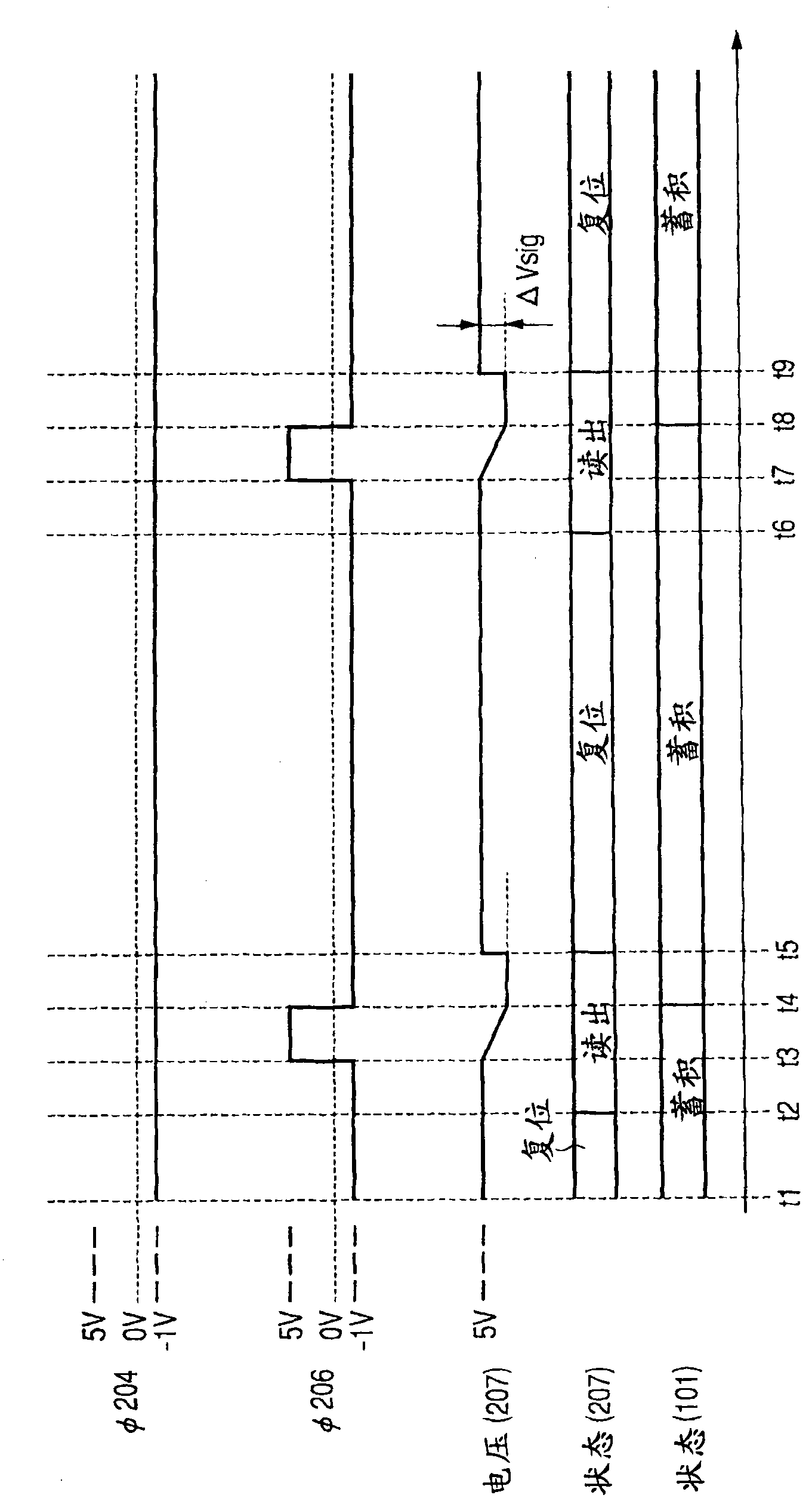
[0040] The difference between this embodiment and the first embodiment is that the control signal Also, in the configuration of the first embodiment, the first semiconductor region and the fourth semiconductor region differ in the relationship between their potentials. Figure 5 shows a timing diagram of operation, and, Figure 6 schematically shows with when according to Figure 5 The potential corresponding to the signal charge in each semiconductor region when driving is performed. Figure 5 and image 3 correspond, Figure 6A , Figure 6B , Figure 6C and Figure 6D and Figure 4A , Figure 4B , Figure 4C and Figure 4D correspond, and similar functions are denoted by similar symbols, and descriptions thereof are omitted.

[0041] First, in Figure 5 , the control signal is not always low, and goes high at t3 (and at t7). control signal When the signal charge from the photoelectric conversion element 101 is transferred to a high level, it is possible to s...

no. 3 example

[0047] The difference between this embodiment and the second embodiment is that the control signal The low level and the control signal The low level is different. In this embodiment, the control signal The low level is set to -3V, while the control signal The low level is set to -1V. That is, the low level of the voltage supplied to the second gate electrode is higher than the low level of the voltage supplied to the first gate electrode. This voltage-to-voltage relationship can increase the breakdown voltage between the second gate electrode 206 and the third semiconductor region 207 . The reason is as follows. The third semiconductor region 207 is set to a high potential at reset. At this time, if a low-level voltage is supplied to the first gate electrode 204 and the second gate electrode 206 , the electric field between the adjacent second gate electrode 206 and the third semiconductor region 207 increases. Then, making the low-level voltage of the second gate ...


PUM


Abstract

A photoelectric conversion apparatus includes: a first semiconductor region forming a part of a photoelectric conversion element; a second semiconductor region stacked on the first semiconductor region, and forming a part of the photoelectric conversion element; a third semiconductor region to which a signal charge transferred from the photoelectric conversion element; a fourth semiconductor region of the first conductivity type having an higher impurity concentration, between the first and third semiconductor region and between the second and third semiconductor regions, closer to a main surface than the first semiconductor region, and connected to the first semiconductor region; a first gate electrode over the fourth semiconductor region, an insulating film on the main surface and between the first gate electrode and the fourth semiconductor region; and a second gate electrode between the third and fourth semiconductor regions, and over the insulating film.

Description

technical field [0001] The present invention relates to a photoelectric conversion device, and more particularly, to a transfer structure of signal charges from a photoelectric conversion element. Background technique [0002] Conventionally, a known photoelectric conversion device includes a device that transfers charge of a photoelectric conversion element to a floating diffusion region through a transfer MOS transistor and converts it into a voltage for readout. [0003] Regarding such a photoelectric conversion device, Japanese Patent Application Laid-Open No. 2004-063498 discloses a configuration in which signal charges are read out at a low voltage and do not leave signal charges. Specifically, it is a photoelectric conversion device including a first gate electrode approximately close to one end of the photodiode region, a second gate electrode close to the first gate electrode, and a drain region approximately close to one end of the second gate electrode. [0004] ...

Claims


Application Information

Patent Timeline
Patent Type & Authority Patents(China)
IPC IPC(8): H01L27/146H04N5/335H04N5/341H04N5/357H04N5/369H04N5/374
CPCH01L27/14603H01L27/14643H01L27/14609H01L27/14605
Inventor 山下雄一郎
Owner CANON KK
Why Eureka
Try Eureka