Liquid crystal display panel and manufacturing method thereof

A liquid crystal display panel and liquid crystal technology, applied in nonlinear optics, instruments, optics, etc., can solve the problems of reducing the utilization rate of ultraviolet light, achieve the effect of improving the utilization rate of ultraviolet light and reducing the probability of failure

Active Publication Date: 2017-02-15
BEIJING BOE OPTOELECTRONCIS TECH CO LTD
View PDF3 Cites 1 Cited by
  • Summary
  • Abstract
  • Description
  • Claims
  • Application Information

AI Technical Summary

Problems solved by technology

During the UV curing process of the sealant, ultraviolet light can be incident from the side of the CF substrate, and the incident ultraviolet light is transmitted from the sealant coated on the array substrate to the outside of the LCD panel, and this part of the transmitted ultraviolet light cannot be continuously used , thus reducing the utilization rate of ultraviolet light

Method used


Image

  • Liquid crystal display panel and manufacturing method thereof
  • Liquid crystal display panel and manufacturing method thereof
  • Liquid crystal display panel and manufacturing method thereof

Examples


Embodiment 1

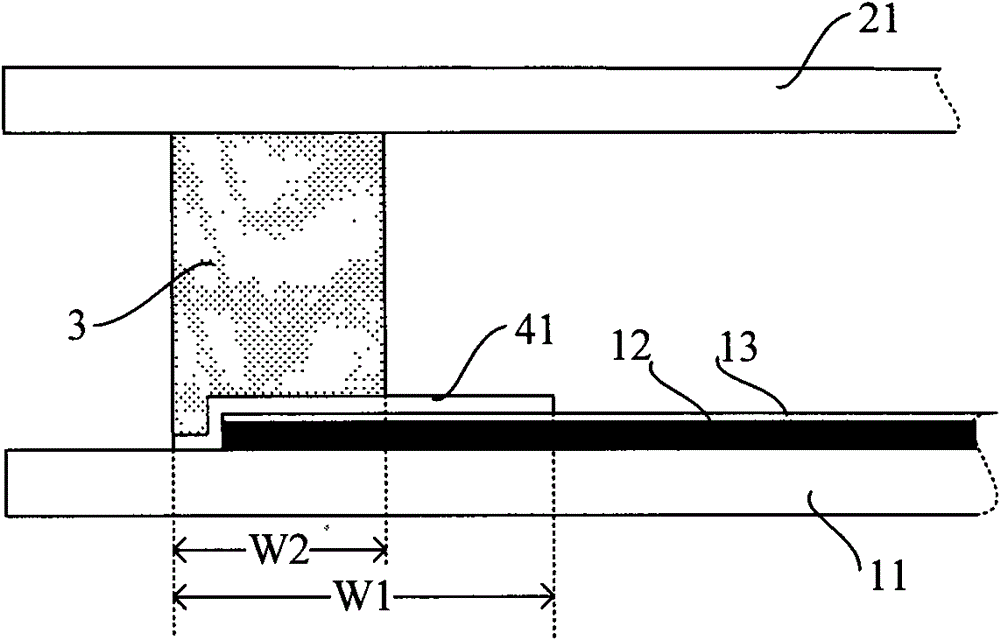
[0027] figure 1 It is a schematic diagram of the structure of the peripheral region of the LCD panel provided by the first embodiment of the present invention. In this embodiment, a light-reflecting layer (hereinafter referred to as the first light-reflecting layer) is formed on a side of the peripheral area of ​​the CF substrate facing the sealant, that is, the first light-reflection layer and the sealant are located on the same side of the CF substrate. Such as figure 1 As shown, the liquid crystal display panel of this embodiment includes: a CF substrate and an array substrate, and the CF substrate and the array substrate are arranged opposite to each other up and down.

[0028] The array substrate mainly includes: a second transparent substrate 21 and an array structure pattern formed on the second transparent substrate 21 . The array structure pattern is the same as that of the prior art. For example, the array structure pattern (not shown) includes: a gate line pattern...

Embodiment 2

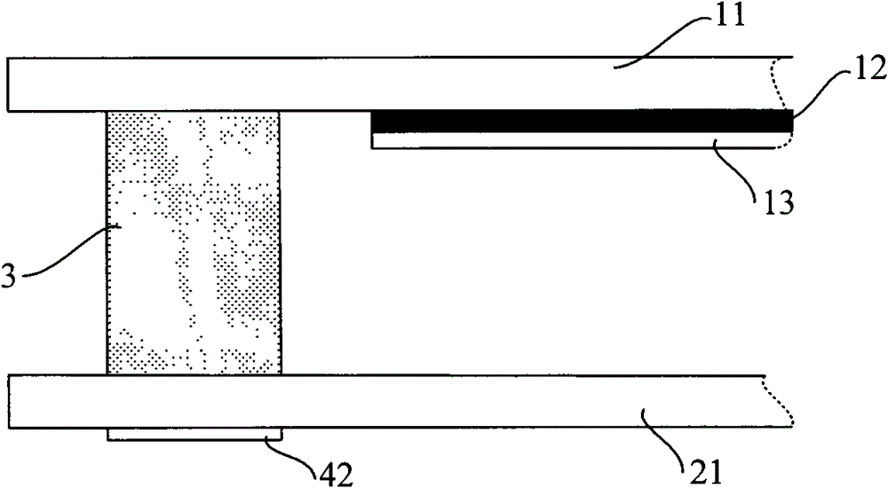
[0041] figure 2 It is a schematic diagram of the structure of the peripheral area of ​​the LCD panel provided by the second embodiment of the present invention. Such as figure 2 As shown, the difference between the LCD panel of this embodiment and the LCD panel of the first embodiment of the present invention is that the LCD panel of this embodiment is formed with a reflective layer (hereinafter referred to as the first Two reflective layers 42 ), that is, the second reflective layer 42 and the sealant 3 are located on two opposite sides of the array substrate. Specifically, the second reflective layer 42 and the array pattern are respectively formed on two opposite surfaces of the second transparent substrate 21, the second reflective layer 42 is formed on the side of the second transparent substrate 21 close to the backlight source, and at least partially covers the The array substrate is used for coating or aligning the corresponding area of ​​the sealant 3 to reflect t...

Embodiment 3

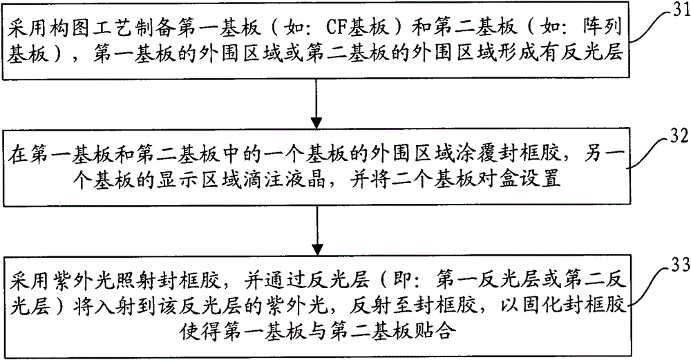
[0055] image 3 It is a flow chart of the manufacturing method of the LCD panel provided by the third embodiment of the present invention. Such as image 3 As shown, the manufacturing method of the LCD panel of the present embodiment includes:

[0056] Step 31: Prepare the first substrate (such as CF substrate) and the second substrate (such as array substrate) by patterning process, the peripheral area of ​​the first substrate or the peripheral area of ​​the second substrate is formed with a reflective layer.

[0057] For TFT-LCD, the two substrates that make up the LCD panel are: CF substrate and array substrate. It may be advisable to use the CF substrate as the first substrate in this embodiment, and use the array substrate as the second substrate in this embodiment.

[0058] If a reflective layer (that is, the first reflective layer) is formed on the peripheral area of ​​the CF substrate, the first reflective layer is formed on the side of the peripheral area of ​​the ...


PUM

PropertyMeasurementUnit
thicknessaaaaaaaaaa
thicknessaaaaaaaaaa

Abstract

A liquid crystal display panel and a manufacturing method thereof are provided. The liquid crystal display panel comprises: a first substrate and a second substrate bonded to each other; a liquid crystal layer filled between a display region of the first substrate and a display region of the second substrate; and a sealant formed between a periphery region of the first substrate and a periphery region of the second substrate. A reflective layer is formed in the periphery region of the first substrate or in the periphery region of the second substrate, and the reflective layer is adapted to reflect UV light to the sealant in a process of assembling the first substrate and the second substrate.

Description

technical field [0001] The invention relates to the field of display technology, in particular to a liquid crystal display panel and a manufacturing method thereof. Background technique [0002] A liquid crystal display panel for a Thin Film Transistor Liquid Crystal Display (TFT-LCD) mainly includes a color filter (ColorFilter, CF) substrate and an array (Array) substrate, and between the CF substrate and the array substrate. filled liquid crystal layer. The process of setting the pre-prepared CF substrate and the array substrate in the box is called the "box-to-box process". The peripheral area of ​​the first substrate is uniformly coated with sealant; after the coating of the sealant and the liquid crystal dripping are completed, the two substrates are accurately aligned in the box, and the sealant is cured to achieve the lamination of the two substrates. The substrate coated with sealant can be a CF substrate, and the substrate dripped with liquid crystal can be an arr...

Claims


Application Information

Patent Timeline
Patent Type & Authority Patents(China)
IPC IPC(8): G02F1/1333G02F1/1339G02F1/1362G02F1/1368
CPCG02F1/133553G02F1/1339G02F1/133388
Inventor 宋勇志皇甫鲁江罗会月王煦
Owner BEIJING BOE OPTOELECTRONCIS TECH CO LTD
Why Eureka
Try Eureka