Method for manufacturing semiconductor device

A device manufacturing method and technology for manufacturing methods, which are applied in semiconductor/solid-state device manufacturing, electrical components, circuits, etc., and can solve problems such as reducing product reliability.

Inactive Publication Date: 2011-04-20
SEMICON MFG INT (SHANGHAI) CORP
View PDF1 Cites 11 Cited by
  • Summary
  • Abstract
  • Description
  • Claims
  • Application Information

AI Technical Summary

Problems solved by technology

With the continuous reduction of the critical dimension of semiconductor devices, especially after entering the 90nm and higher-level process, the metal oxide 111 will cause the "electromigration" phenomenon of the top metal layer 101, reducing the reliability of the product

Method used


Image

  • Method for manufacturing semiconductor device
  • Method for manufacturing semiconductor device
  • Method for manufacturing semiconductor device

Examples


Embodiment Construction

[0045] The invention provides a method for manufacturing a semiconductor device. An annealing process is performed after the formation of the protective layer, which eliminates or reduces the remaining pinholes in the protective layer, and prevents oxygen from passing through the remaining pinholes when the photoresist is removed by ashing. Oxidation is caused to the top metal layer, which avoids the electromigration phenomenon caused by it, and improves the reliability of the device.

[0046] In order to make the methods, features and advantages of the present invention more comprehensible, the specific implementation manners of the present invention will be described in detail below in conjunction with the accompanying drawings.

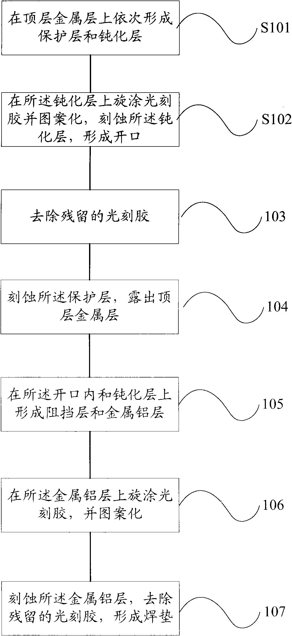
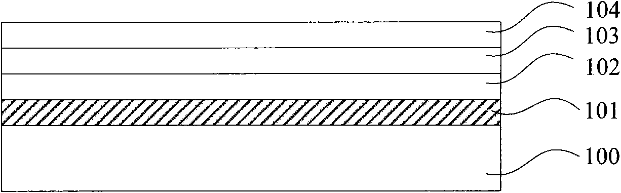
[0047] Figure 11 It is a schematic flow chart of a pad manufacturing method according to an embodiment of the present invention, Figure 12 to Figure 2 2 is a schematic cross-sectional structure diagram of a method for manufacturing a pad accordi...


PUM

PropertyMeasurementUnit
thicknessaaaaaaaaaa

Abstract

The invention discloses a method for manufacturing a semiconductor device, which comprises: providing a substrate, wherein a top metal layer is formed on the surface of the substrate; forming a protective layer on the top metal layer; annealing the protective layer; forming a passivated layer on the protective layer; photoetching and etching the passivated layer to form a solder pad opening; forming a barrier layer and a metal aluminum layer in the solder pad opening and on the passivated layer; and photoetching and etching the metal aluminum layer to form a solder pad. In the invention, residual needle holes in the protective layer are eliminated or reduced, oxidization of the top metal layer by oxygen passing through the needle holes during ashing photoresist removal is prevented, and electromigration problem thus caused is avoided.

Description

technical field [0001] The invention relates to the technical field of semiconductors, in particular to a manufacturing method of a semiconductor device. Background technique [0002] In the semiconductor manufacturing process, after completing the manufacturing process of the semiconductor device in the front-end process and the metal interconnection line in the back-end process, it is necessary to form a protective layer and a passivation layer on the top metal layer to achieve moisture resistance and pressure resistance. the goal of. In order to realize the electrical connection with the inside of the device, it is necessary to form openings in the passivation layer and the protective layer, fill the openings with metal, and make pads to lead out the power lines or signal lines inside the device. In the subsequent packaging process , the outer leads are soldered to the pads or solder bumps are formed on the pads. Metal aluminum has the advantages of low resistivity, eas...

Claims


Application Information

Patent Timeline
Patent Type & Authority Applications(China)
IPC IPC(8): H01L21/60
Inventor 金泰圭辛永基
Owner SEMICON MFG INT (SHANGHAI) CORP
Why Eureka
Try Eureka