Check patentability & draft patents in minutes with Patsnap Eureka AI!

Electrostatic discharge protection circuit

An electrostatic discharge protection and circuit technology, used in emergency protection circuit devices, emergency protection circuit devices for limiting overcurrent/overvoltage, circuits, etc. Open and other problems to achieve good uniformity

Inactive Publication Date: 2011-04-20
GRACE SEMICON MFG CORP
View PDF0 Cites 12 Cited by
  • Summary
  • Abstract
  • Description
  • Claims
  • Application Information

AI Technical Summary

Problems solved by technology

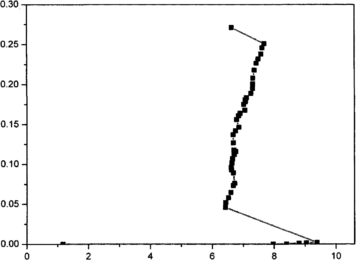
[0009] To sum up, in the above ESD protection circuit, only some of the first NPNs in the middle part are discharging. Since the voltage cannot be higher than the trigger voltage (9.1V) of the NPN, until these NPNs are burned, the NPNs on both sides are also discharged. It cannot be turned on normally, and thus cannot be discharged, so it cannot play the role of ESD protection

Method used


Image

  • Electrostatic discharge protection circuit
  • Electrostatic discharge protection circuit
  • Electrostatic discharge protection circuit

Examples


Embodiment Construction

[0037] In order to make the above objects, features and advantages of the present invention more comprehensible, specific implementations of the present invention will be described in detail below in conjunction with the accompanying drawings.

[0038] see Figure 4 , the figure is the prior art figure 2 corresponding layout.

[0039] from Figure 4 It can be seen that the circle around the layout is figure 2 B in

[0040] In the middle of the layout are multiple NMOS transistors connected in parallel.

[0041] see Figure 5 , which is the layout of the ESD protection circuit composed of multi-finger NMOS transistors according to the present invention.

[0042] Compare Figure 5 with Figure 4 , it can be clearly seen that the difference between the present invention and the prior art is that the parallel multi-finger NMOS transistors are grouped, and each group includes at least one NMOS transistor; the surroundings of each group of NMOS transistors are surrounded b...


PUM


Abstract

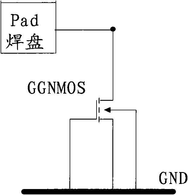
The invention relates to an electrostatic discharge protection circuit which comprises a plurality of NMOS (N-type metal-oxide semiconductor) tubes, and gates of the NMOS tubes are grounded and connected in parallel; a drain of each NMOS tube is connected with a bonding pad (Pad), the gates are grounded, sources are grounded, and substrates are grounded; the NMOS tubes are grouped, and each group comprises at least one NMOS tube; and the periphery of the NMOS tube of each group is surrounded by a P-well in a contact manner. The invention relates to the electrostatic discharge protection circuit which comprises a plurality of NFOD (N-type field oxide device) tubes connected in parallel; a drain of each NFOD tube is connected with the bonding pad (Pad), the sources are grounded, and the substrates are grounded; the NFOD tubes are grouped, and each group comprises at least one NFOD tube; and the periphery of the NFOD tube of each group is surrounded by the P-well in a contact manner. Therefore, the difference between parasitic NPN (negative-positive-negative) base resistance positioned at the middle and the parasitic NPN base resistance positioned on two sides in each group is smaller, when ESD (electrostatic discharge) pulses are added on a PAD (portable application description) for generating drain current which flows into the base resistance, all NPN base-emitters are positively biased, and all NPN are in uniform conduction.

Description

technical field [0001] The invention relates to the technical field of electrostatic discharge, and particularly designs an electrostatic discharge protection circuit. Background technique [0002] As the manufacturing process of integrated circuits enters the era of deep sub-micron line width, the MOS elements in integrated circuits adopt lightly doped drain (LDD, Lightly Doped Drain) structure, and the silicide process has been widely used in the diffusion layer of MOS elements superior. At the same time, in order to reduce the diffusion series resistance of the gate polycrystal, a polycrystal compound manufacturing process is adopted. With the shrinking of integrated circuit components, the thickness of the gate oxide layer of MOS components is getting thinner and thinner. The improvement of these manufacturing processes can greatly increase the operation speed inside the integrated circuit and increase the integration level of the circuit. However, these improvements h...

Claims


Application Information

Patent Timeline
IPC IPC(8): H01L27/04H01L29/06H01L23/60H02H9/00
CPCH01L2924/0002
Inventor 单毅何军
Owner GRACE SEMICON MFG CORP
Features
  • R&D
  • Intellectual Property
  • Life Sciences
  • Materials
  • Tech Scout
  • Unparalleled Data Quality
  • Higher Quality Content
  • 60% Fewer Hallucinations
Learn More