Array field effect transistor

A field-effect transistor, array-type technology, applied in the direction of electric solid-state devices, semiconductor devices, semiconductor/solid-state device parts, etc., can solve the problems of limited length of the interconnection well 202, which is difficult to meet, and improve the conduction of static charges. Ability, effect of increasing contact length

Active Publication Date: 2011-04-20
SHANGHAI HUAHONG GRACE SEMICON MFG CORP
View PDF0 Cites 2 Cited by
  • Summary
  • Abstract
  • Description
  • Claims
  • Application Information

AI Technical Summary

Problems solved by technology

[0009] The existing finger field effect transistor has the following problem: since the contact length between the diffusion region 100 and the interconnection well 202 is much smaller than the contact length with the channel well 201, and the length of the interconnection well 202 is limited, the above-mentioned parasitic diode conducts The ability of the charge is difficult to meet the requirement of conducting and releasing the static charge in the diffusion region 100 when the device is working, and an additional dedicated diode is required for electrostatic protection

Method used


Image

  • Array field effect transistor
  • Array field effect transistor
  • Array field effect transistor

Examples


Embodiment Construction

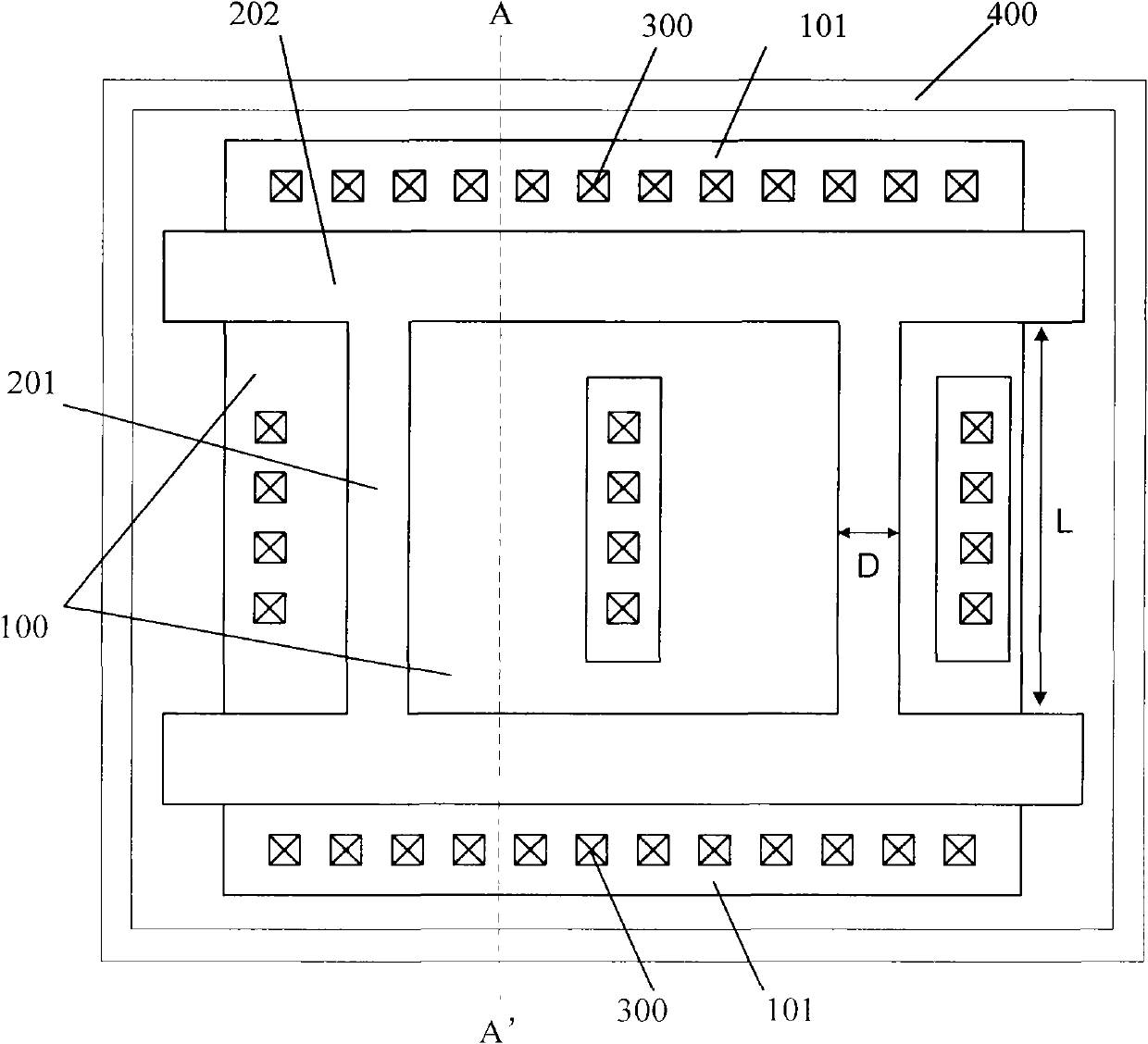
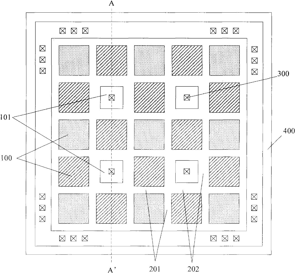
[0028] It can be seen from the background technology that in the existing finger-shaped field effect transistors, the interconnection well and the interconnection region are located on both sides of the diffusion region arranged in parallel, and the contact length between the diffusion region and the interconnection well is the longest of the entire field effect transistor area. The two sides of the diffusion region are long, so the parasitic diodes only exist on both sides of the diffusion region. However, the present invention arranges the diffusion regions and the interconnection regions in an array, so that the channel wells between adjacent diffusion regions and the interconnection wells between adjacent diffusion regions and interconnection regions form a network of “wells” The well line can greatly increase the contact length between the diffusion region and the interconnection well without reducing the channel width.

[0029] The array type field effect transistor prov...


PUM


Abstract

The invention relates to an array field effect transistor. The array field effect transistor is characterized by comprising a silicon on insulator (SOI) substrate and well lines, diffusion regions and interconnection regions which are formed on the SOI substrate, wherein the diffusion regions and the interconnection regions are distributed in an array mode and are spaced by the groined well lines; and the conductive type of the well lines is the same as that of the interconnection regions and is opposite to that of the diffusion regions. Compared with the prior art, the invention has the advantages that: an array structure is formed by the diffusion regions and the interconnection regions, so that on the premise of not reducing the contact length of the diffusion regions and interconnection wells, namely the channel width of a metal-oxide-semiconductor field effect transistor (MOSFET), the array field effect transistor greatly increases the contact length of the diffusion regions and the interconnection wells, improves the capacity of conducting electrostatic charges of parasitic diodes between the diffusion regions and the interconnection wells, meets the requirements that the electrostatic charges in the diffusion regions are released when a device works and is suitable for electrostatic protection of the small-size device.

Description

technical field [0001] The invention relates to the field of integrated circuit layout (layout), in particular to an array type field effect transistor based on silicon on insulator (SOI). Background technique [0002] In field effect transistors, in order to eliminate secondary effects such as substrate bias, it is often necessary to fix the potential of the well region of the field effect transistor; in addition, in the I / O unit circuit of the integrated circuit, it is also necessary to consider the static electricity in the circuit release problem; therefore, in the layout design of integrated circuits, it is necessary to lead out the well region of the field effect transistor to ground, and further, connect the drawn interconnection line to the static elimination circuit and then ground to eliminate static electricity. [0003] The application of silicon-on-insulator to make substrates has become one of the hot spots in the field of integrated circuit manufacturing in re...

Claims


Application Information

Patent Timeline
Patent Type & Authority Applications(China)
IPC IPC(8): H01L27/12H01L23/528H01L29/78H01L29/06
CPCH01L2924/0002
Inventor 何军
Owner SHANGHAI HUAHONG GRACE SEMICON MFG CORP
Why Eureka
Try Eureka