Organic electroluminescence device with stable luminescence and preparation method thereof

A stable and luminescent technology, which is applied in the fields of electrical solid-state devices, semiconductor/solid-state device manufacturing, electrical components, etc.

Inactive Publication Date: 2011-04-20
UNIV OF ELECTRONICS SCI & TECH OF CHINA
View PDF3 Cites 54 Cited by
  • Summary
  • Abstract
  • Description
  • Claims
  • Application Information

AI Technical Summary

Problems solved by technology

[0005] The problem to be solved by the present invention is: how to provide an organic electroluminescent device with stable

Method used


Image

  • Organic electroluminescence device with stable luminescence and preparation method thereof
  • Organic electroluminescence device with stable luminescence and preparation method thereof
  • Organic electroluminescence device with stable luminescence and preparation method thereof

Examples


Embodiment 1

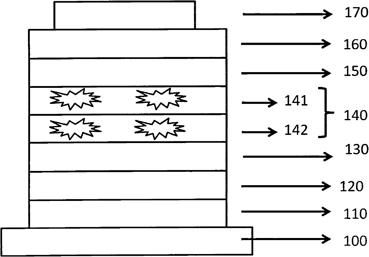
[0057] like figure 1 As shown, the substrate 100 of the device is a glass substrate, the first electrode layer 110 is an ITO anode, 120 is a hole injection layer, 130 is a hole transport layer, and the light emitting layer 140 in the structure of the device is a composite doped light emitting layer , 150 is an electron transport layer, 160 is an electron injection layer, and 170 is a cathode.

[0058] The hole injection material of the device is 2-TNATA, the material of the hole transport layer is NPB, the host material in the first doped light-emitting layer is NPB, the guest material is the blue phosphorescent material FIrpic with a doping concentration of 50wt%, and the second doped The host material of the heteroluminescent layer is TPBi, the guest material is the blue phosphorescent material FIrpic with a doping concentration of 8wt%, the electron transport material is TPBi, and the electron injection material is Alq 3 , The cathode layer is made of Mg:Ag alloy. The ent...

Embodiment 2

[0068] like figure 1 As shown, the substrate 100 of the device is a flexible substrate PET, the first electrode layer 110 is a polymer anode PANI, 120 is a hole injection layer, 130 is a hole transport layer, and the light emitting layer 140 in the structure of the device is a composite doped In the miscellaneous light-emitting layer, 150 is an electron transport layer, 160 is an electron injection layer, and 170 is a cathode.

[0069] The hole injection material of the device is 2-TNATA, the material of the hole transport layer is NPB, the host material of the first doped light-emitting layer is NPB, the guest material is DCM2 with a doping concentration of 3wt% red fluorescent material, and the second doped light-emitting layer The host material is TPBi, the guest material is DCM2 with a doping concentration of 3wt% red fluorescent material, the electron transport material is TPBi, and the electron injection material is Alq 3 , The cathode layer is made of Mg:Ag alloy. The...

Embodiment 3

[0079] like figure 1 As shown, the substrate 100 of the device is a glass substrate, the first electrode layer 110 is an ITO anode, 120 is a hole injection layer, 130 is a hole transport layer, and the light emitting layer 140 in the structure of the device is a composite doped light emitting layer , 150 is an electron transport layer, 160 is an electron injection layer, and 170 is a cathode.

[0080] The hole injection material of the device is DNTPD, the material of the hole transport layer is TCTA, the host material of the first doped light-emitting layer is TCTA, and the guest material is the green fluorescent material Ir(ppy) with a doping concentration of 5wt%. 3 , the host material of the second doped light-emitting layer is PBD, and the guest material is the green fluorescent material Ir(ppy) with a doping concentration of 5wt%. 3 , the electron transport material is PBD, the electron injection material is BPhen, and the cathode layer uses Mg:Ag alloy. The entire dev...


PUM

PropertyMeasurementUnit
Sheet resistanceaaaaaaaaaa
Film thicknessaaaaaaaaaa

Abstract

The invention claims an organic electroluminescence device with stable luminescence, which comprises a substrate, a first electrode layer, a functional layer and a second electrode. The first electrode layer is arranged on the surface of the substrate; the functional layer is arranged on the first electrode layer and the second electrode is arranged above the functional layer, wherein the functional layer at least comprises an electron injection layer, an electronic transmission layer, a luminous layer, a hole transmission layer and a hole injection layer; the luminous layer is a compound doping luminous layer consisting of a double-layer doping luminous layer; the double-layer doping luminous layer respectively uses electronic transmission materials and hole transmission materials as a main material. By adopting the conventional phosphorescence dyes and fluorescent dyes with excellent performance as doping object materials in the luminous layer, through adjusting the thickness and the components of the luminous layer, the invention prepares the organic electroluminescence device with stable luminescence and high performance to meet the use requirement on information display and illumination.

Description

technical field [0001] The invention relates to the field of organic photoelectric technology in electronic components, in particular to an organic electroluminescent device with stable light emission and a preparation method thereof. Background technique [0002] An organic electroluminescent device (Organic Light-Emitting Device, OLED) is a photoelectric device using an organic solid-state semiconductor as a light-emitting material, and its light-emitting mechanism is electroluminescence (EL for short). Its structure is as figure 1 As shown, it includes a substrate 100, an anode electrode 110, a hole injection layer (Hole Injection Layer) 120, a hole transport layer (Hole Transport Layer, HTL) 130, a composite doped light emitting layer 140, an electron transport layer (Electron Transport Layer) ) 150, electron transport layer (Electron Transport Layer) 160 and cathode electrode 170. When a forward bias voltage is applied to the cathode and anode, electrons and holes wil...

Claims


Application Information

Patent Timeline
IPC IPC(8): H01L51/50H01L51/56
Inventor 蒋亚东于军胜张伟余双江
Owner UNIV OF ELECTRONICS SCI & TECH OF CHINA
Why Eureka
Try Eureka