Low-voltage SCR (Silicon Controlled Rectifier) structure for ESD (Electronic Static Discharge) protection of integrated circuit chip

An ESD protection and integrated circuit technology, applied in the electronic field, can solve the problems of reduced ESD resistance, increased voltage drop, chip failure, etc., to achieve excellent ESD protection performance, low trigger voltage, and fast trigger speed.

Inactive Publication Date: 2011-04-27
UNIV OF ELECTRONICS SCI & TECH OF CHINA
View PDF3 Cites 21 Cited by
  • Summary
  • Abstract
  • Description
  • Claims
  • Application Information

AI Technical Summary

Problems solved by technology

Using SCR devices can get a strong anti-ESD ability, but when the chip is working normally, due to external interference, the SCR may be falsely triggered, causing a latch-up effect (latch-up), resulting in chip failure
In order to avoid this phenomenon, the method of increasing the maintenance voltage of SCR is often used to make the maintenance voltage higher than the power supply voltage, but increasing the maintenance voltage will increase the voltage drop on the LVTSCR when the ESD current is discharged, and then increase the power consumption. Therefore, it tends to reduce the ESD resistance of the device
This is also the design difficulty of using SCR as an ESD protection device

Method used


Image

  • Low-voltage SCR (Silicon Controlled Rectifier) structure for ESD (Electronic Static Discharge) protection of integrated circuit chip
  • Low-voltage SCR (Silicon Controlled Rectifier) structure for ESD (Electronic Static Discharge) protection of integrated circuit chip
  • Low-voltage SCR (Silicon Controlled Rectifier) structure for ESD (Electronic Static Discharge) protection of integrated circuit chip

Examples


specific Embodiment approach 1

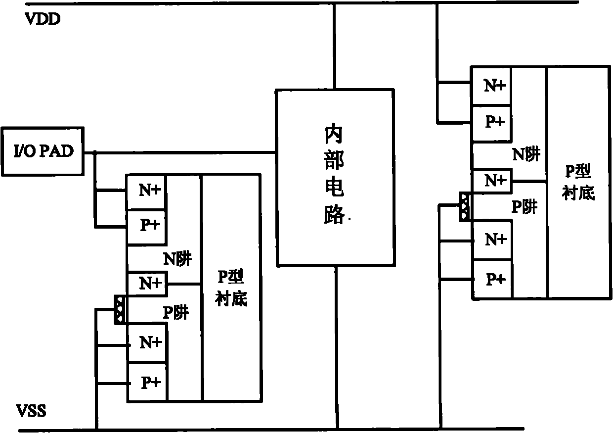
[0037] A low-voltage SCR structure used for ESD protection of integrated circuit chips, such as Figure 4 As shown, two types of low-voltage SCR ESD protection devices are included, and the two types of SCR ESD protection devices are integrated on the same chip substrate with the integrated circuit chips they protect.

[0038] The first type of low-voltage SCR ESD protection device includes an N well region, two P well regions, three P + area and the four N + region, the N well region is sandwiched between two P well regions; the middle of the top of the first P well region is the first N well region + region, the side of the top of the first P well region far away from the N well region is the first P + region; the middle of the top of the second P well region is the second N + region, the side of the top of the second P well region away from the N well region is the second P well region + region; the middle of the top of the N well region is the third P + District; Thir...

specific Embodiment approach 2

[0040] Such as Figure 5 shown in Figure 4 On the basis of the technical scheme shown, the third and fourth polysilicon regions are added above the N well region of the first type of low-voltage SCR ESD protection device; the third polysilicon region is located in the third N well region + District and Third P + above the N well region between regions, the fourth polysilicon region is located in the fourth N + District and Third P + Above the N well region between the regions, there is an insulating layer between the third and fourth polysilicon regions and the N well region; I / O ports are connected. The third and fourth polysilicon regions are added above the P well region of the second type of low-voltage SCR ESD protection device; the third polysilicon region is located in the third P + District and Third N + above the P well region between regions, the fourth polysilicon region is located in the fourth P + District and Third N + Above the P well region between the...

specific Embodiment approach 3

[0041] Such as Image 6 shown in Figure 4 On the basis of the technical scheme shown, the third and fourth polysilicon regions are added above the N well region of the first type of low-voltage SCR ESD protection device; the third polysilicon region is located in the third N well region + District and Third P + above the N well region between regions, the fourth polysilicon region is located in the fourth N + District and Third P + Above the N well region between the regions, there is an insulating layer between the third and fourth polysilicon regions and the N well region; The VDD rail of the power rails is connected. The third and fourth polysilicon regions are added above the P well region of the second type of low-voltage SCR ESD protection device; the third polysilicon region is located in the third P + District and Third N + above the P well region between regions, the fourth polysilicon region is located in the fourth P + District and Third N + Above the P wel...


PUM


Abstract

The invention relates to a low-voltage SCR (Silicon Controlled Rectifier) structure for ESD (Electronic Static Discharge) protection of an integrated circuit chip, belonging to the technical field of electronics. The structure comprises two kinds of low-voltage SCR ESD protection devices, wherein the first kind of SCR ESD protection device integrates two N-well diodes and two NMOSs (N-channel Metal Oxide Semiconductors); the N-well diodes are connected between I/O (Input/Output) and a VDD (Virtual Device Driver); the NMOSs are connected between the VDD and VSS (Visual Source Safe); and the N-well diodes and the NMOSs form an SCR structure which provides ESD protection between PS and PD modes and VDD-VSS. The second kind of device integrates two P-well diodes and two PMOSs (P-channel Metal Oxide Semiconductors), wherein the P-well diodes are connected between the I/O and the VSS, and the PMOSs are connected between the VSS and the VDD, and the P-well diodes and the PMOSs jointly form an SCR structure which provides ESD protection between ND and NS modes and VDD-VSS. According to the invention, the chip has higher maintaining voltage and latch-up resistance effect during normal working and has lower triggering voltage and higher triggering speed during ESD; and the low-voltage SCR structure can effectively reduce the relative chip-occupying area of the protection devices and decrease parasitic capacitance at the same time of providing a plurality of modes of ESD protection functions and excellent ESD protection performance.

Description

technical field [0001] The invention belongs to the field of electronic technology, and relates to the design technology of an electrostatic discharge (ESD for short) protection circuit of a semiconductor integrated circuit chip, in particular to a single control circuit to control multiple protection devices, so that the protection devices can be timely and effectively Discharge the ESD current, and at the same time save the silicon chip area occupied by the control circuit. Background technique [0002] Electrostatic discharge is a common phenomenon in the process of manufacturing, producing, assembling, testing, storing, and transporting semiconductor devices or circuits. The pin is passed into the integrated circuit and destroys the internal circuit of the integrated circuit. In order to solve this problem, a protection circuit is usually placed next to the I / O pin during chip design. The protection circuit must be activated before the electrostatic discharge pulse dama...

Claims


Application Information

Patent Timeline
Patent Type & Authority Applications(China)
IPC IPC(8): H01L27/02H02H9/00
CPCH01L29/87
Inventor 蒋苓利樊航张波刘娟喻钊
Owner UNIV OF ELECTRONICS SCI & TECH OF CHINA
Why Eureka
Try Eureka