Method for preventing uneven surface of wafer and preventing defocus in exposure

A technology with uneven surface and wafers, which is applied in the manufacturing of photosensitive materials, electrical components, semiconductor/solid-state devices for optomechanical equipment, etc., and can solve problems such as uneven thickness of wafers

Inactive Publication Date: 2011-05-04
SEMICON MFG INT (SHANGHAI) CORP +1
View PDF1 Cites 7 Cited by
  • Summary
  • Abstract
  • Description
  • Claims
  • Application Information

AI Technical Summary

Problems solved by technology

[0006] The problem to be solved by the present invention is to provide a method for preventing unevenness of the wafer surface and defocusing during exposure, avoiding ...

Method used


Image

  • Method for preventing uneven surface of wafer and preventing defocus in exposure
  • Method for preventing uneven surface of wafer and preventing defocus in exposure
  • Method for preventing uneven surface of wafer and preventing defocus in exposure

Examples


Embodiment Construction

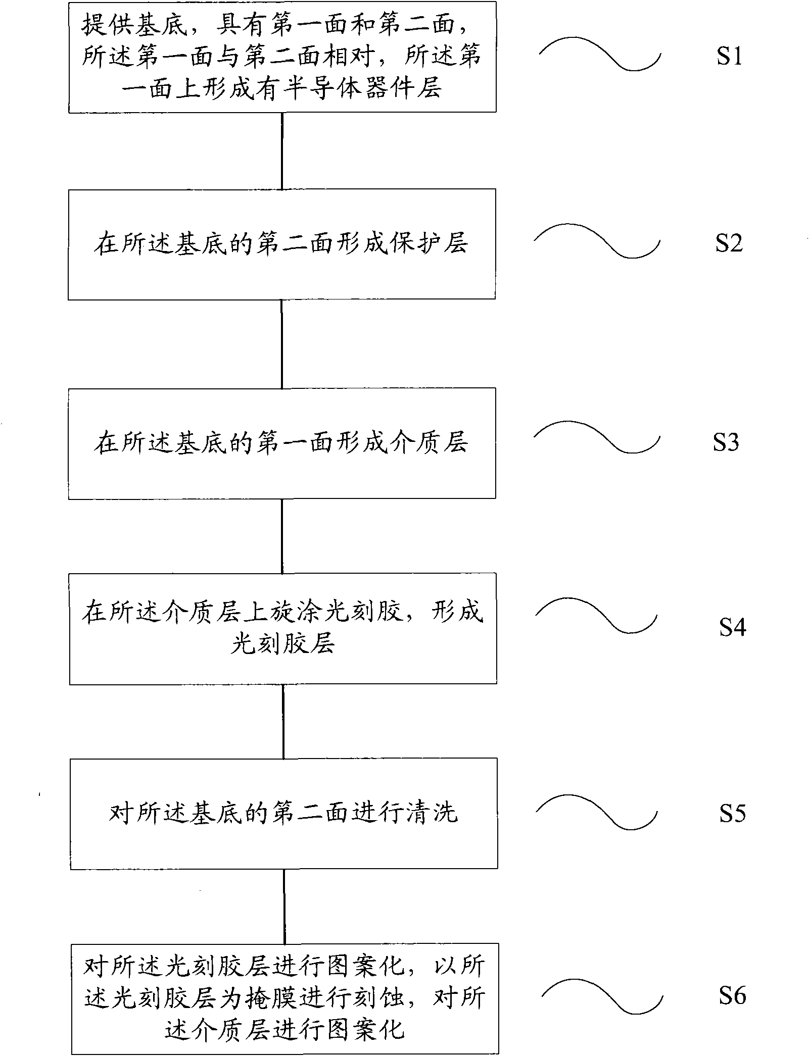
[0030] The invention provides a method for preventing unevenness of the wafer surface and loss of focus during exposure. A protective layer is formed on the back of the wafer, which avoids the uneven thickness of the wafer caused by the cleaning and polishing process, and prevents the out of focus problem.

[0031] In order to make the methods, features and advantages of the present invention more comprehensible, the specific implementation manners of the present invention will be described in detail below in conjunction with the accompanying drawings.

[0032] The present invention provides a method for preventing the surface of a wafer from being uneven, comprising: providing a substrate, the substrate has a first surface and a second surface, the first surface is opposite to the second surface, and the first surface is formed with A semiconductor device layer; forming a protective layer on the second surface of the base. Taking the etching of the dielectric layer on the su...


PUM

PropertyMeasurementUnit
Thicknessaaaaaaaaaa

Abstract

The invention provides a method for preventing uneven surface of a wafer, comprising the following steps: providing a substrate, wherein the substrate comprises a first surface and a second surface, the first surface is corresponding to the second surface and the first surface is formed with a semiconductor device layer; and then forming a protective layer on the second surface of the substrate. A method for preventing defocus in exposure, comprising the following steps: providing a substrate, wherein the substrate comprises a first surface and a second surface, the first surface is corresponding to the second surface and the first surface is formed with a semiconductor device layer; forming a protective layer on the second surface of the substrate; forming a photoresist layer; and then exposing the photoresist layer. The method for preventing uneven surface of a wafer and preventing defocus in exposure provided by the invention has the advantages that the phenomenon of uneven thickness of the wafer during the cleaning process is prevented and the defocus problem in photoresist exposure is prevented.

Description

technical field [0001] The invention relates to the technical field of semiconductor manufacturing, in particular to a method for preventing wafer surface unevenness and out-of-focus during exposure. Background technique [0002] In the semiconductor manufacturing process, photolithography and etching processes are widely used. The process of photolithography mainly includes forming a photoresist layer; using a photolithography machine to pattern the photoresist layer; The glue layer is used as a mask for etching; after etching, the remaining photoresist is removed. With the continuous improvement of the technology level, the feature size (CD, critical dimension) of the device is continuously reduced, especially after entering the 90nm process, the focus problem in the patterning process of the photoresist layer becomes more and more important. The defocus phenomenon will seriously reduce the yield of the manufacturing process. [0003] In the U.S. Patent No. 5780204, a me...

Claims


Application Information

Patent Timeline
IPC IPC(8): H01L21/314G03F7/09
Inventor 周鸣刘焕新
Owner SEMICON MFG INT (SHANGHAI) CORP
Why Eureka
Try Eureka