Semiconductor device structure and manufacturing method thereof

A technology of device structure and manufacturing method, applied in semiconductor/solid-state device manufacturing, semiconductor devices, semiconductor/solid-state device components, etc., can solve problems such as discharge phenomenon excitation, test failure, etc., to avoid lattice defects and device damage Effect

Active Publication Date: 2011-05-04
CSMC TECH FAB2 CO LTD
View PDF1 Cites 3 Cited by
  • Summary
  • Abstract
  • Description
  • Claims
  • Application Information

AI Technical Summary

Problems solved by technology

[0009] In the existing process of forming interconnection lines, when the conductive plug is formed by etching, the residual charge brought by plasma etching will gradually accumulate in the metal wiring layer, and the discharge phenomenon will be excited under certain conditions, resulting in Discharge occurs between the metal wiring layer and the semiconductor substrate, making the test invalid

Method used


Image

  • Semiconductor device structure and manufacturing method thereof
  • Semiconductor device structure and manufacturing method thereof
  • Semiconductor device structure and manufacturing method thereof

Examples


Embodiment 1

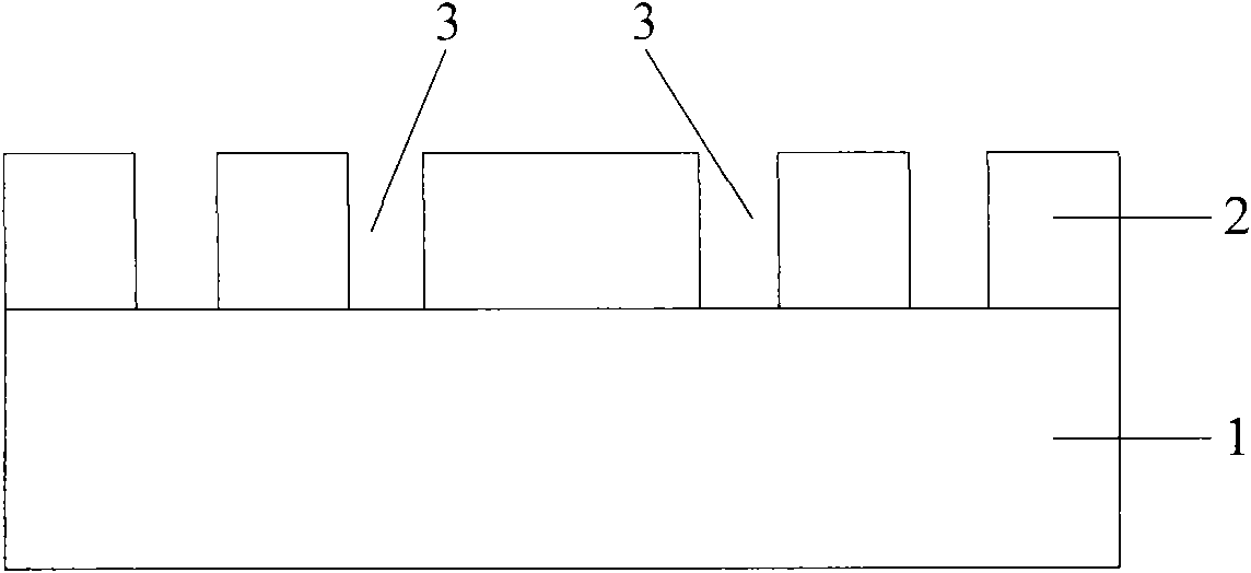
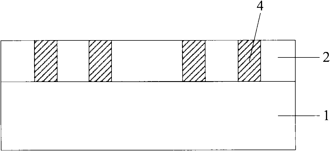
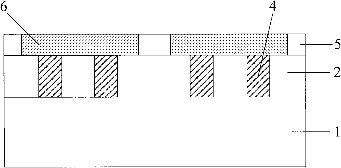
[0027] Figures 6 to 9 It is a schematic diagram of a first embodiment of forming an interconnection structure using the present invention. like Image 6 As shown, a semiconductor substrate 100 is provided, and the semiconductor substrate 100 may be a logic structure with multiple layers of metal lines, or may be a metal line layer on the surface of a logic structure; wherein the semiconductor substrate 100 is divided into device regions II and dummy region I at the edge of the semiconductor substrate. A first insulating layer 102 with a thickness of less than 10,000 angstroms is formed on the surface of the semiconductor substrate 100 by chemical vapor deposition, and the first insulating layer 102 acts as an electrical isolation to ensure that the current of the formed semiconductor product only flows through the interconnection lines .

[0028] In this embodiment, the material of the first insulating layer 102 may be silicon oxide.

[0029] continue to refer to Image ...

Embodiment 2

[0044] Figures 10 to 13 It is a schematic diagram of a second embodiment of forming an interconnection structure using the present invention. like Figure 10 As shown, a semiconductor substrate 200 is provided, and the semiconductor substrate 200 may be a logic structure with multiple layers of metal lines, or may be a metal line layer on the surface of a certain layer of logic structure; wherein the semiconductor substrate 200 is divided into device regions II and dummy region I at the edge of the semiconductor substrate. A first insulating layer 202 with a thickness of less than 10,000 angstroms is formed on the surface of the semiconductor substrate 200 by chemical vapor deposition, and the first insulating layer 202 acts as an electrical isolation to ensure that the current of the formed semiconductor product only flows through the interconnection lines .

[0045] In this embodiment, the material of the first insulating layer 202 may be silicon oxide.

[0046] continu...


PUM


Abstract

The invention provides a semiconductor device structure and a manufacturing method thereof. The semiconductor device structure comprises a semiconductor substrate, a plurality of insulating layers, a plurality of metal wiring layers, conductive plugs in a device region and conductive plugs in a virtual region, wherein the semiconductor substrate is divided into the device region and the virtual region; the virtual region is arranged on the edge of the semiconductor substrate; one insulating layer is arranged on the semiconductor substrate; the metal wiring layers are formed among the insulating layers; the conductive plugs in the device region are arranged in each insulating layer and penetrate through the insulating layer in the thickness direction, and are used for connecting the metal wiring layers; and the conductive plugs in the virtual region are arranged in one insulating layer and penetrate through the insulating layer in the thickness direction, and are used for directly connecting any metal wiring layer with the semiconductor substrate. The invention has the following advantage: the electric charges accumulated in the metal wiring layers and the insulating layers during etching are timely released, thus avoiding lattice defects and device damage caused by residual electric charges.

Description

technical field [0001] The present invention relates to the field of manufacture of semiconductor devices, in particular to a structure of a semiconductor device for releasing accumulated charges through a dummy conductive plug connected to a semiconductor substrate and a method for manufacturing the same. Background technique [0002] With the rapid development of ULSI (Ultra Large Scale Integration) technology, miniaturization of the wiring design principles of semiconductor devices is progressing. The number of components to be integrated is increasing, the wiring of large-scale integrated circuits is more complex, and the metal wiring is becoming thinner, narrower, and thinner. In this case, multi-layer interconnection has attracted attention, and contact hole conductive plug deposition is a key interconnection technology. Interconnect technology plays a key role in improving product yield. [0003] At present, when manufacturing semiconductor products, a common interc...

Claims


Application Information

Patent Timeline
Patent Type & Authority Applications(China)
IPC IPC(8): H01L23/528H01L23/60H01L21/768
CPCH01L23/52H01L23/585H01L2924/0002
Inventor 谢宝强朱旋肖玉洁杨兆宇
Owner CSMC TECH FAB2 CO LTD
Why Eureka
Try Eureka