Annealing treatment method for Al-0.5Cu conducting layer

A technology of annealing treatment and conductive layer, which is applied in the field of annealing treatment of conductive materials, can solve the problems of metal short circuit, affecting yield, short circuit, etc., and achieve the effect of avoiding growth and protrusion and increasing yield

Inactive Publication Date: 2011-05-11
HEJIAN TECH SUZHOU
View PDF0 Cites 0 Cited by
  • Summary
  • Abstract
  • Description
  • Claims
  • Application Information

AI Technical Summary

Problems solved by technology

The copper-rich region is difficult to be completely etched in the subsequent etching process, and the remaining part of the copper will cause a short circuit between the metallines, affecting the electrical performance of the wafer and reducing its yield.
[0004] In a high-temperature and high-vacuum environment, the annealing treatment can melt the precipitated copper back into the Al-0.5Cu conductive layer, but the existing annealing treatment tends to cause the growth and protrusion of Al particles in the conductive layer, and the growth and protrusion of Al are the same. It will make it difficult to be completely etched in the subsequent etching process, resulting in short circuits and problems affecting yield

Method used


Image

  • Annealing treatment method for Al-0.5Cu conducting layer
  • Annealing treatment method for Al-0.5Cu conducting layer
  • Annealing treatment method for Al-0.5Cu conducting layer

Examples


Embodiment 1

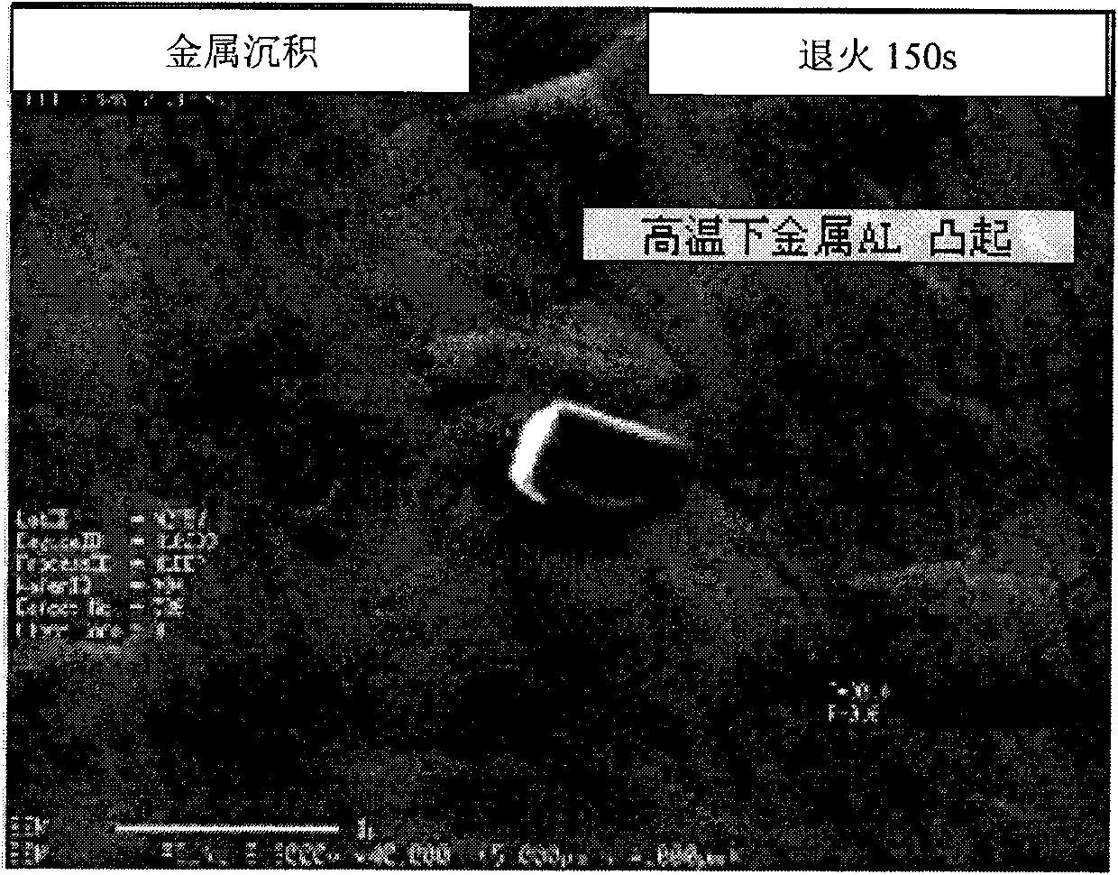
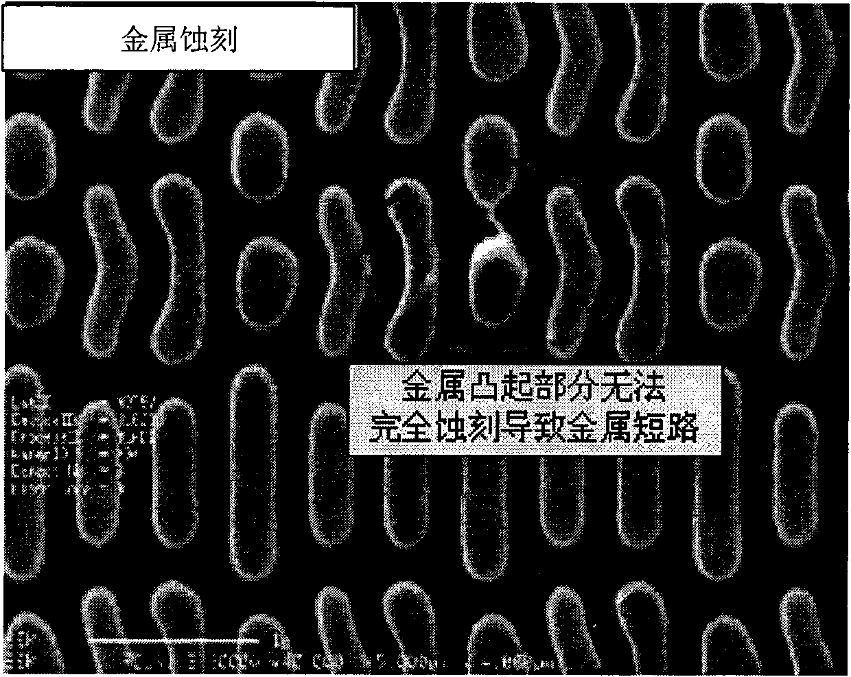
[0024] Set the thickness to The Al-0.5Cu conductive layer wafer was placed in a high-vacuum annealing furnace at a temperature of 420°C for 150s, and then cooled to room temperature at 7°C / s for subsequent etching. Figure 1A It is the SEM picture of the conductive layer obtained after 150s annealing treatment. It can be seen from the figure that there are obvious protrusions on the surface of the Al-0.5Cu conductive layer after annealing, and the outer periphery of the protrusions has very clear edges and corners, indicating that the Al particles have The tendency to aggregate grows. During the etching process, since the protrusion is difficult to etch completely, such as Figure 1B As shown in Fig. 1, there are irregular substances between the metals after etching, which eventually lead to short circuits.

Embodiment 2

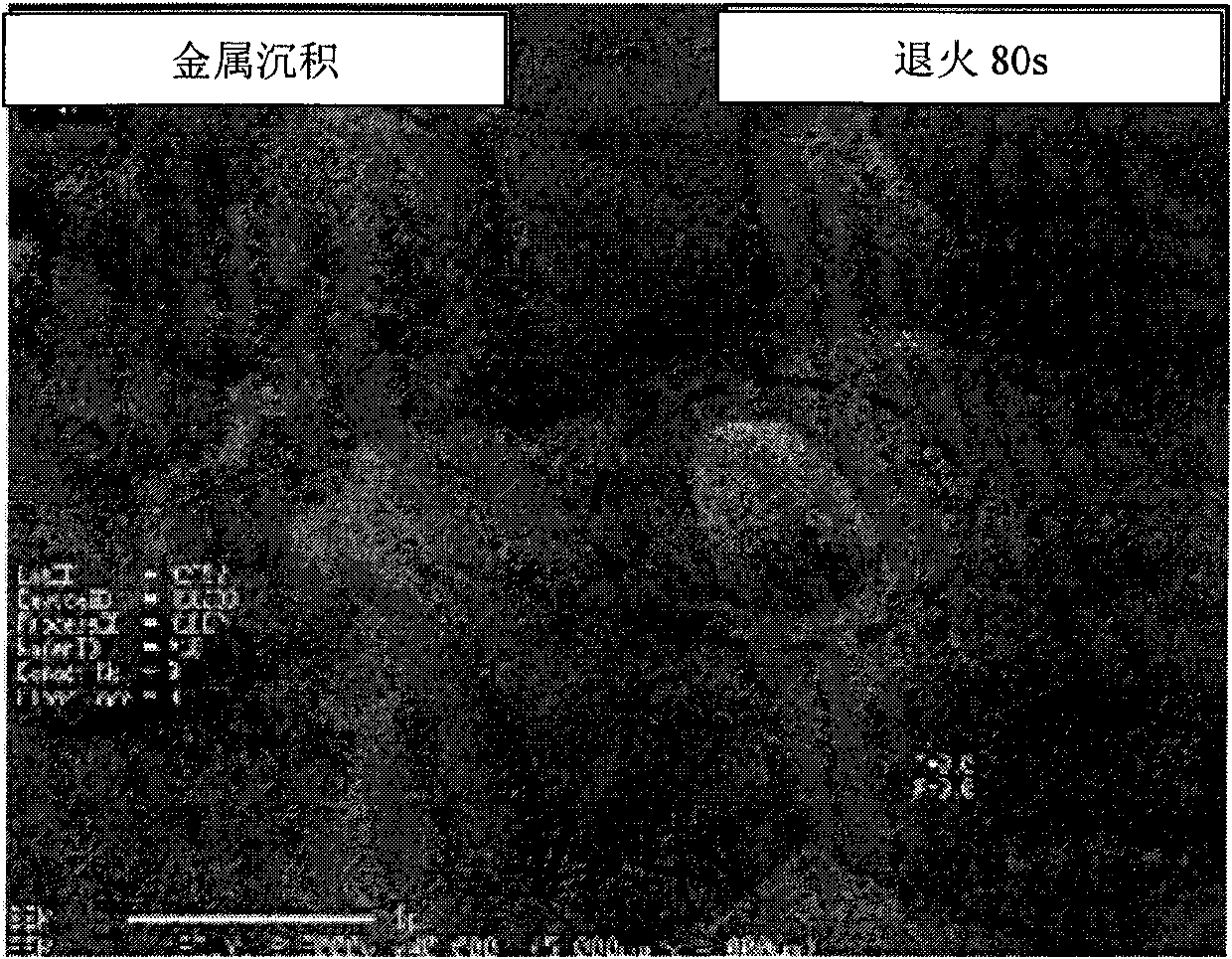
[0026] Set the thickness to The Al-0.5Cu conductive layer wafer was placed in a high-vacuum annealing furnace at a temperature of 420°C for 80s, and then cooled to room temperature at 7°C / s for the subsequent etching process. Compared with Example 1, this example shortens the holding time of the annealing treatment under other conditions being the same. Figure 2A It is the SEM image of the wafer obtained after the 80s annealing treatment, as can be seen from the figure, the Al-0.5Cu conductive layer surface after the annealing is not very smooth, there is a small part of protrusions, but compared with embodiment 1, its periphery is smoother . It shows that under this condition, most of the copper melts back into the alloy material, no obvious copper-rich region is formed, and no obvious Al particle protrusion occurs. So, after performing the post-etch process, such as Figure 2B As shown in the SEM image, the morphology is good, and there is no short circuit phenomenon ca...

Embodiment 3

[0029] Set the thickness to The Al-0.5Cu conductive layer wafer was placed in a high-vacuum annealing furnace at a temperature of 380°C for 150s, and then cooled to room temperature at 12°C / s for subsequent etching. Figure 3A It is the SEM image of the conductive layer obtained after the 150s annealing treatment. As can be seen from the figure, the surface of the Al-0.5Cu conductive layer after annealing has obvious protrusions, similar to Example 1, and the outer peripheral edges and corners of the protrusions are also relatively clear. It shows that Al particles tend to aggregate and grow. During the etching process, since the protrusion is difficult to etch completely, such as Figure 3B As shown in Fig. 1, there are irregular substances between the metals after etching, which eventually lead to short circuits.


PUM


Abstract

The invention provides an annealing treatment method for an Al-0.5Cu conducting layer. The conducting layer is arranged into a high-vacuum environment, is remained for a period of time at the temperature of 380-420DEG C and is cooled; and when the thickness of the Al-0.5Cu conducting layer is 2500 to 8000 angstroms, annealing time is 60-300s, and the annealing time is prolonged with the increase of the thickness of the Al-0.5Cu conducting layer. Under the annealing treatment condition provided by the annealing treatment method, copper can be melted back to Al-0.5Cu alloy material and can be dispersed in the alloy material so as to overcome the problem of copper precipitation. Meanwhile, annealing time in the annealing treatment process of different Al-0.5Cu conducting layers is controlled to prevent Al particles from growing and extruding, thereby avoiding the short circuit of wafers and improving the yield.

Description

technical field [0001] The invention relates to a method for annealing a conductive material, in particular to a method for annealing an Al-0.5Cu conductive layer in an IC manufacturing process. Background technique [0002] In the field of IC (integrated circuit) manufacturing, Al-0.5Cu alloy material is widely used in chip conductive layer. In the Al-0.5Cu alloy material, the doping of Cu element can weaken the electromigration and improve the service life of the chip. [0003] However, locally saturated Cu will precipitate from the alloy crystal phase, forming copper-rich regions. The copper-rich region is difficult to be completely etched in the subsequent etching process, and the remaining copper will cause a short circuit between metallines, which will affect the electrical performance of the wafer and reduce its yield. [0004] In a high-temperature and high-vacuum environment, the annealing treatment can melt the precipitated copper back into the Al-0.5Cu conductiv...

Claims


Application Information

Patent Timeline
Patent Type & Authority Applications(China)
IPC IPC(8): C21D1/26C21D11/00C22F1/057
Inventor 徐忠良周烽
Owner HEJIAN TECH SUZHOU
Why Eureka
Try Eureka