Display and thin film transistor array substrate and thin film transistors thereof

A technology of thin-film transistors and array substrates, applied in the field of display devices, can solve the problems of general products and methods without suitable structures and methods, inconvenience, and increased manufacturing process costs of reflective displays, so as to shorten the manufacturing process time and save manufacturing processes cost effect

Active Publication Date: 2011-05-11
E INK HLDG INC
View PDF2 Cites 3 Cited by
  • Summary
  • Abstract
  • Description
  • Claims
  • Application Information

AI Technical Summary

Problems solved by technology

However, in order to avoid leakage current from the thin film transistor 101 in this way, it is necessary to add an additional photomask in the manufacturing process of the reflective display, and thus increase the cost of the manufacturing process of the reflective display.
[0008] It can be seen that the above-mentioned existing displays and thin film transistor array substrates and thin film transistors obviously still have inconvenience and defects in product structure, manufacturing method (processing method) and use, and need to be further improved urgently.
In order to solve the above-mentioned problems, the relevant manufacturers have tried their best to find a solution, but no suitable design has been developed for a long time, and there is no suitable structure and method for general products and methods to solve the above-mentioned problems. This is obviously a problem that relevant industry players are eager to solve

Method used


Image

  • Display and thin film transistor array substrate and thin film transistors thereof
  • Display and thin film transistor array substrate and thin film transistors thereof
  • Display and thin film transistor array substrate and thin film transistors thereof

Examples


Embodiment Construction

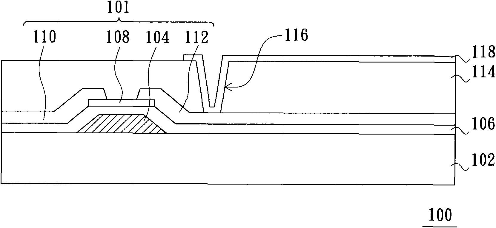
[0053] In order to further explain the technical means and effects of the present invention to achieve the intended purpose of the invention, the following, in conjunction with the accompanying drawings and preferred embodiments, will describe the specific implementation of the display and its thin film transistor array substrate and thin film transistor according to the present invention. Structure, method, step, feature and effect thereof are as follows in detail.

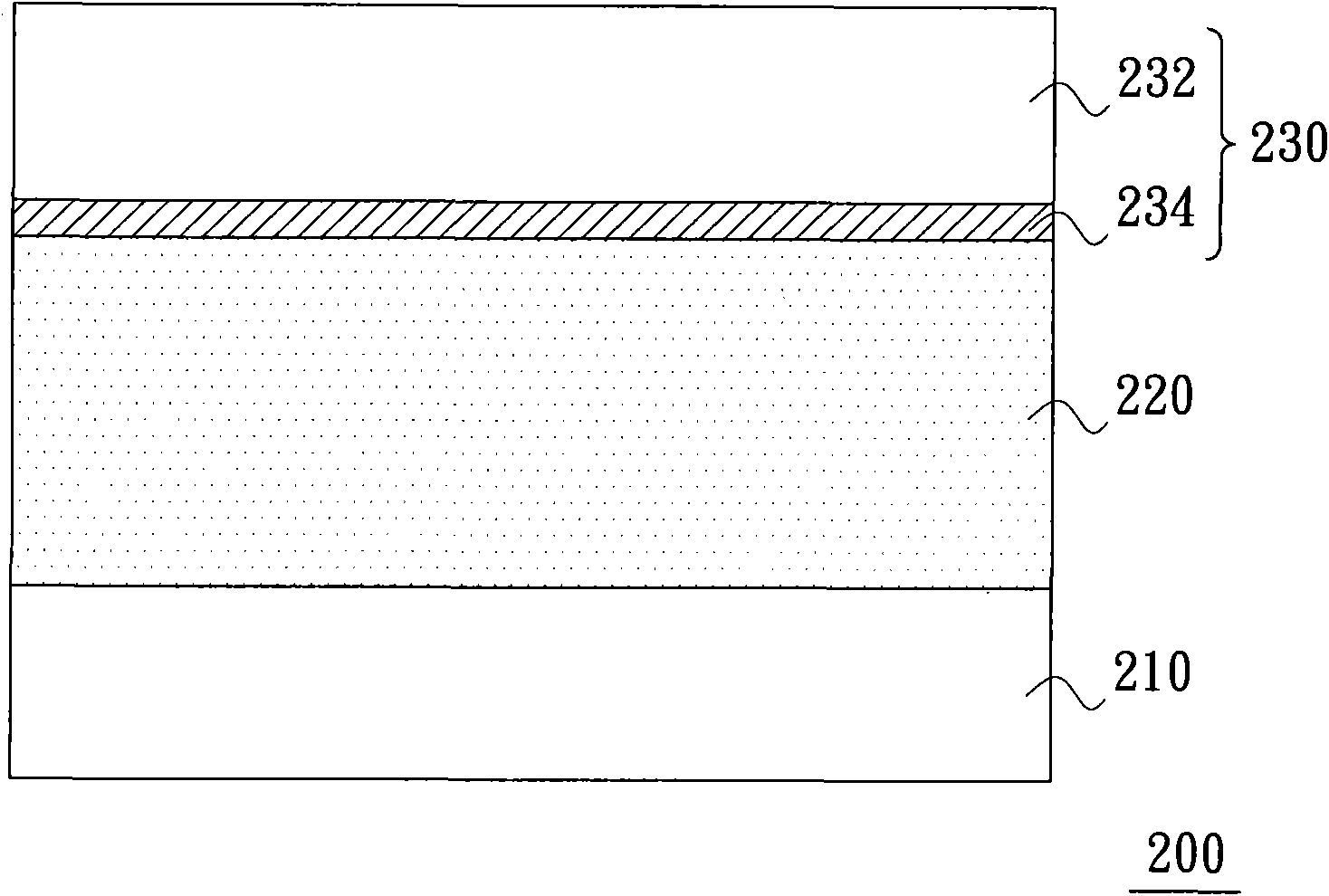
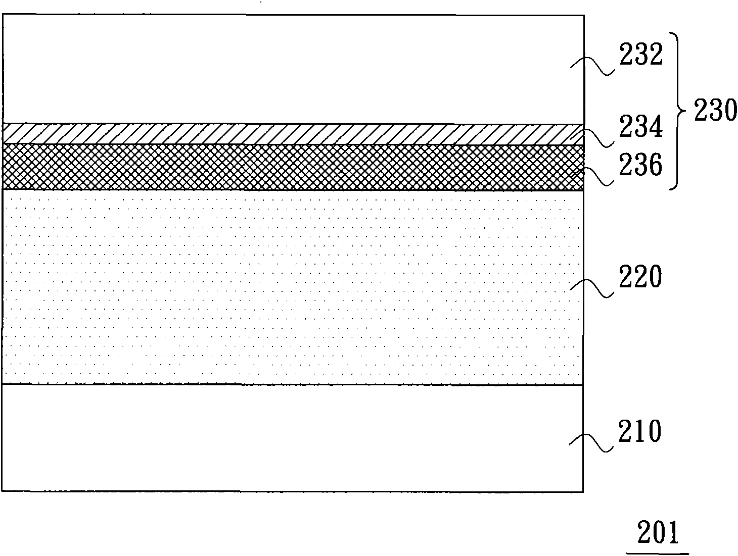
[0054] figure 2 It is a schematic cross-sectional view of a display in an embodiment of the present invention. Please refer to figure 2 The display 200 includes a thin film transistor array substrate 210, a display medium layer 220 and a transparent electrode substrate 230, wherein the transparent electrode substrate 230 is located above the thin film transistor array substrate 210, and the display medium layer 220 is arranged on the transparent electrode substrate 230 and the transparent electrode substrate 2...


PUM


Abstract

The invention relates to a display and a thin film transistor array substrate and thin film transistors thereof. The display comprises the thin film transistor array substrate, an optically transparent electrode substrate and a display dielectric layer arranged between the thin film transistor array substrate and the optically transparent electrode substrate, wherein the thin film transistor array substrate comprises a plurality of thin film transistors with oxide semiconductor layers; grid electrodes and grid insulating layers of the thin film transistors are arranged on the substrate respectively; the grid electrodes are covered by the grid insulating layers; the oxide semiconductor layers cover on the grid insulating layers conformally and are provided with channel regions positioned above the grid electrodes; and source electrodes and drain electrodes of the thin film transistors are arranged on the oxide semiconductor layers respectively and are positioned on the two sides of each channel region. The oxide semiconductor layers are made of optically transparent materials, so that a manufacturing process for patterning the oxide semiconductor layers can be eliminated in a display manufacturing process so as to save manufacturing cost and shorten the time of the manufacturing process.

Description

technical field [0001] The present invention relates to a display device, in particular to a display with a thin film transistor that does not generate leakage current due to illumination, a thin film transistor array substrate and a thin film transistor. Background technique [0002] A reflective display uses reflected incident light as a light source for displaying images on the display. Since the reflective display does not need to be equipped with a backlight source, the power consumption of the components is reduced, and the entire display can be designed to be thinner and lighter, so it has been highly valued in the display industry in recent years. [0003] On the other hand, most current displays can be classified into active and passive according to their driving components. Generally, active displays mostly use thin film transistors as driving components, and because the manufacturing process of amorphous silicon thin film transistors (a-Si TFTs) is simple and low...

Claims


Application Information

Patent Timeline
Patent Type & Authority Applications(China)
IPC IPC(8): H01L29/786H01L29/24H01L27/02G09F9/00
Inventor 舒芳安陈礼廷王裕霖蓝纬洲林东亮
Owner E INK HLDG INC
Why Eureka
Try Eureka