Optical proximity correction method

An optical proximity effect and area technology, applied in the field of photolithography, can solve the problems of reducing production efficiency and increasing the running time of the optical proximity effect correction system, etc.

Inactive Publication Date: 2011-05-18
CSMC TECH FAB1 +1
View PDF1 Cites 12 Cited by
  • Summary
  • Abstract
  • Description
  • Claims
  • Application Information

AI Technical Summary

Problems solved by technology

Although the correction accuracy can be guaranteed in this way, for the twill area and the blank area, the correction accuracy is too high, which increases the running time of the optical proximity effect correction system and reduces the production efficiency.
[0004] The Chinese patent application number 200610024872.7 discloses a pattern segmentation method for correcting the optical proximity effect, but it is only applicable to the segmentation of contact hole patterns, and the criterion for the pattern segmentation is the prohibition distance

Method used


Image

  • Optical proximity correction method
  • Optical proximity correction method
  • Optical proximity correction method

Examples


Embodiment Construction

[0013] The technical solutions and other beneficial effects of the present invention will be apparent through the detailed description of specific embodiments of the present invention below in conjunction with the accompanying drawings.

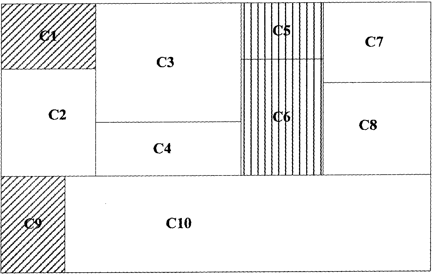
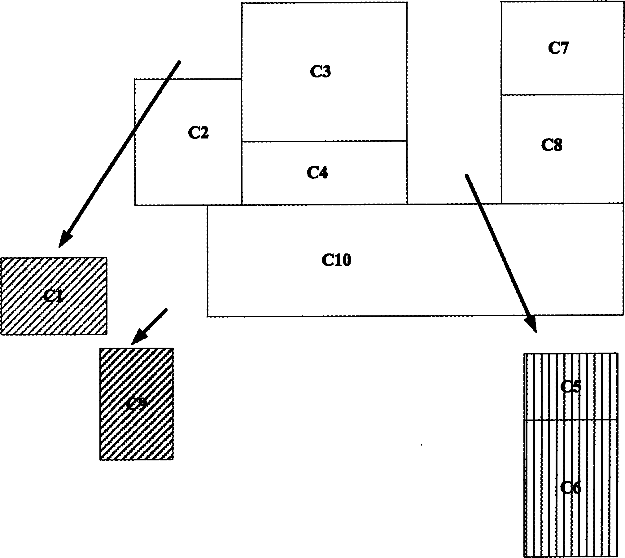
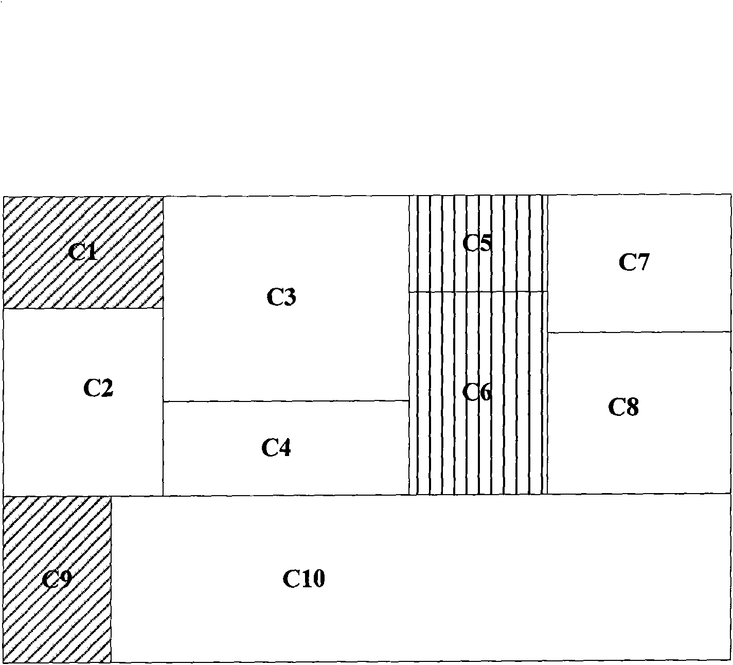
[0014] The optical proximity effect correction method is to divide a layout into multiple regions according to the difference in critical dimension control accuracy. figure 2 is a schematic diagram of the first embodiment of the optical proximity effect correction method. Assume that the vertical bar area (C5, C6) has high requirements for critical dimension control accuracy, the twill area (C1, C9) has medium critical dimension control accuracy requirements, and the blank area (C2, C3, C4, C7, C8, C10) has high requirements for critical dimension control accuracy. The critical dimension control accuracy requirement is low, so the layout is decomposed according to the difference in critical dimension control accuracy. In the preferred decom...


PUM


Abstract

The invention relates to photoetching technology in the semiconductor industry, in particular to an optical proximity correction method. The method comprises the following steps of: dividing a territory into at least two areas according to different critical dimension control accuracies; and respectively performing optical proximity correction on the at least two areas according to the requirement on critical dimension control accuracy, and adopting the same correction accuracy for areas with the same critical dimension control accuracy. By the optical proximity correction method, areas with different critical dimension control accuracies are corrected by using different correction accuracies, the correction accuracy is distributed according to needs, the accuracy requirement of the optical proximity correction is met, the operating time of an optical proximity correction system is effectively shortened, and the production efficiency is improved.

Description

【Technical field】 [0001] The invention relates to photolithography technology in the semiconductor industry, in particular to an optical proximity effect correction method. 【Background technique】 [0002] A layout can be divided into multiple areas according to the control accuracy of critical dimensions (Critical Dimension, CD). When doing optical proximity correction (Optical ProximityCorrection, OPC) on the mask pattern, it is necessary to select different correction precisions to meet the requirements of critical dimension control. However, the higher the accuracy of optical proximity correction, the longer the program takes to run. [0003] See figure 1 , the traditional optical proximity effect correction technology will determine the overall optical proximity effect correction accuracy according to the part that requires the highest critical dimension control accuracy, assuming figure 1 The relationship between the critical dimension control accuracy required by ea...

Claims


Application Information

Patent Timeline
Patent Type & Authority Applications(China)
IPC IPC(8): G03F1/14G03F1/36
Inventor 王谨恒黄旭鑫张雷
Owner CSMC TECH FAB1
Why Eureka
Try Eureka