Substrate-glaring SiC substrate vertical structure light-emitting tube and preparation method thereof
A technology of vertical structure and light-emitting tubes, applied in the direction of electrical components, circuits, semiconductor devices, etc., can solve the problems of high refractive index and low light output rate, improve output power and brightness, overcome high refractive index, and avoid expensive prices Effect
- Summary
- Abstract
- Description
- Claims
- Application Information
AI Technical Summary
Problems solved by technology
Method used
Image

Examples
Embodiment 1
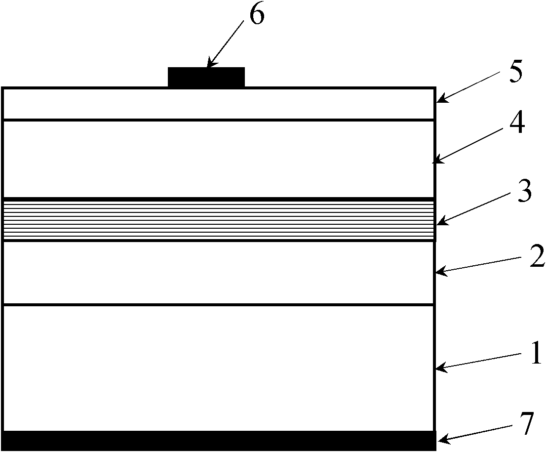
[0032] A new type of substrate light-emitting SiC substrate vertical structure light-emitting tube. The structure of this new type of substrate light-emitting SiC substrate vertical structure light-emitting tube is shown in the appendix figure 2 , sequentially by the substrate 1, the n-type GaN buffer layer epitaxially grown on the substrate 1 and the lower confinement layer 2, the GaN material system multi-quantum well light-emitting layer 3 prepared on the lower confinement layer 2, and the p-type GaN prepared on the light-emitting layer 3 GaN upper confinement layer 4, p-type In prepared on the upper confinement layer 4 x Ga 1-x N cover layer 5, the upper electrode 6 prepared on the cover layer 5, and the lower electrode 7 prepared below the substrate 1 are composed, and it is characterized in that: the upper electrode 6 is prepared to have the function of a reflector concurrently, and at the same time, in order to compensate for the reflection of light on the metal refle...
Embodiment 2
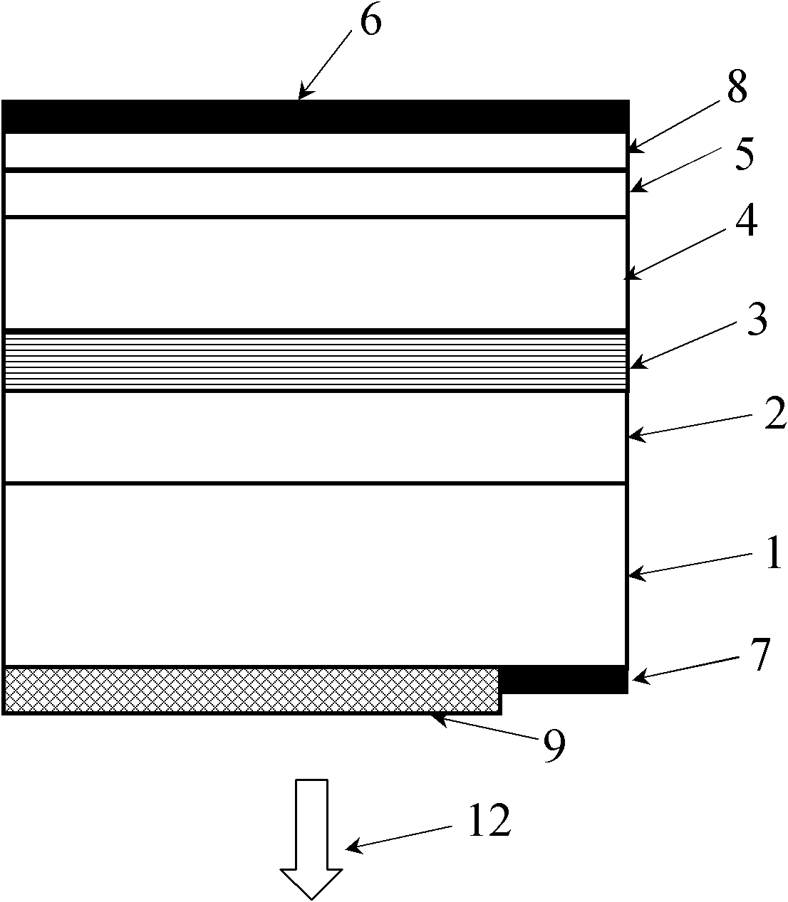
[0035] Transparent dielectric thin film substrate emits light and SiC substrate vertical structure light emitting tube. The structure of this kind of transparent medium film type substrate emits light SiC substrate vertical structure light-emitting tube, see the appendix image 3 , which is characterized in that: the upper electrode 6 is prepared to function as a mirror, and a layer of p-type In is grown between the cap layer 5 and the upper electrode 6 y Ga 1-y The N-phase matching layer 8 and the upper electrode 6 are all covered on the phase matching layer 8 and the cover layer 5. The substrate 1 is an n-type SiC single crystal substrate. A layer of ZnO thin film 9 is prepared under the substrate 1. In order to slow down the ZnO material Refractive index still greatly influences the light output rate, and then prepares a layer of transparent dielectric film 10 with a refractive index between the ZnO material refractive index and the air refractive index under the ZnO film ...
Embodiment 3
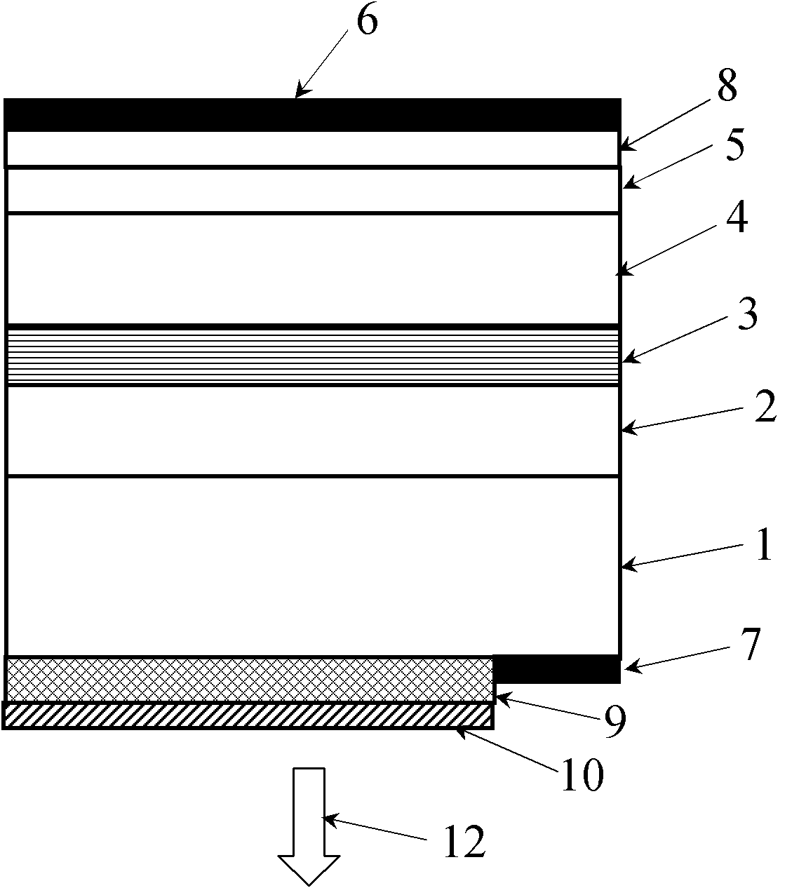
[0038] ZnO nanowire substrate emits light and SiC substrate vertical structure light-emitting tube. This kind of ZnO nanowire substrate emits light and SiC substrate vertical structure light-emitting tube structure is shown in the appendix Figure 4 , which is characterized in that: the upper electrode 6 is prepared to function as a mirror, and a layer of p-type In is grown between the cap layer 5 and the upper electrode 6 y Ga 1-y The N-phase matching layer 8 and the upper electrode 6 are all covered on the phase matching layer 8 and the cover layer 5. The substrate 1 is an n-type SiC single crystal substrate. A layer of ZnO thin film 9 is prepared under the substrate 1. In order to slow down the ZnO material If the refractive index is still high, the light is reflected back to the light-emitting area, which affects the light extraction rate. A layer of ZnO nanowires 11 is prepared under the ZnO film 9, and the electrode 7 is prepared under the substrate 1 only covering 5% t...
PUM
| Property | Measurement | Unit |
|---|---|---|
| thickness | aaaaa | aaaaa |
| thickness | aaaaa | aaaaa |
| thickness | aaaaa | aaaaa |
Abstract
Description
Claims
Application Information
 - R&D
- Intellectual Property
- Life Sciences
- Materials
- Tech Scout
- Unparalleled Data Quality
- Higher Quality Content
- 60% Fewer Hallucinations
Browse by: Latest US Patents, China's latest patents, Technical Efficacy Thesaurus, Application Domain, Technology Topic, Popular Technical Reports.
© 2025 PatSnap. All rights reserved.Legal|Privacy policy|Modern Slavery Act Transparency Statement|Sitemap|About US| Contact US: help@patsnap.com