Bending and forming method of thin silicon wafer

A technology of bending and forming silicon wafers, which is applied in the fields of technology for producing decorative surface effects, decorative art, gaseous chemical plating, etc., can solve the problems of uncontrollable external force forming, easy breakage of silicon wafers, and damage of silicon wafers, etc., to achieve Good bending effect, beneficial to automation, and avoiding damage

Inactive Publication Date: 2011-05-25
DALIAN UNIV OF TECH
View PDF1 Cites 1 Cited by
  • Summary
  • Abstract
  • Description
  • Claims
  • Application Information

AI Technical Summary

Problems solved by technology

[0008] 2. The thickness is single, and only the bending result of 50um thickness is given
Thickness is sensitive to external force. If it is relatively thick, it will be difficult to control the external force forming. If the thickness

Method used


Image

  • Bending and forming method of thin silicon wafer
  • Bending and forming method of thin silicon wafer
  • Bending and forming method of thin silicon wafer

Examples


Embodiment Construction

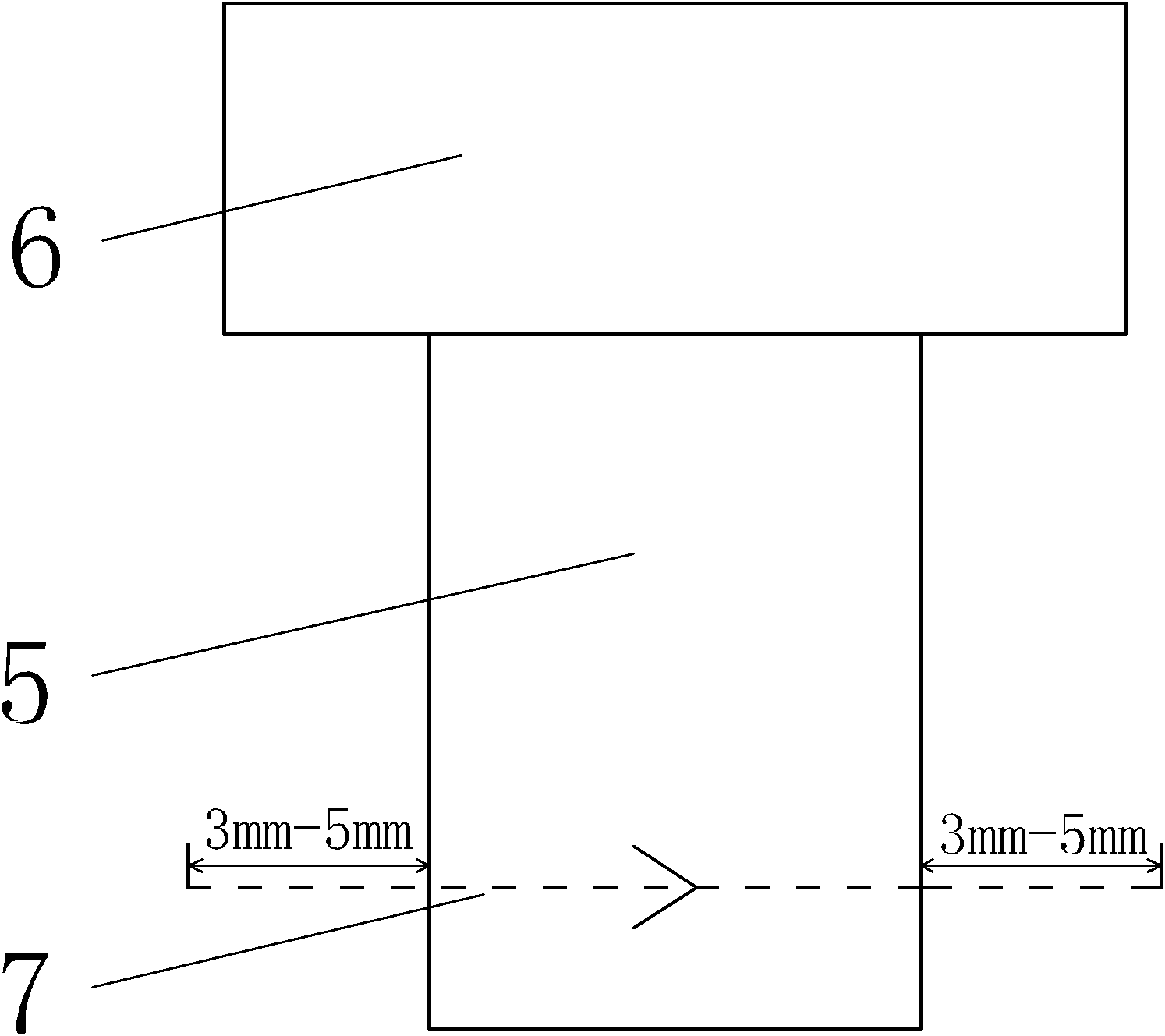
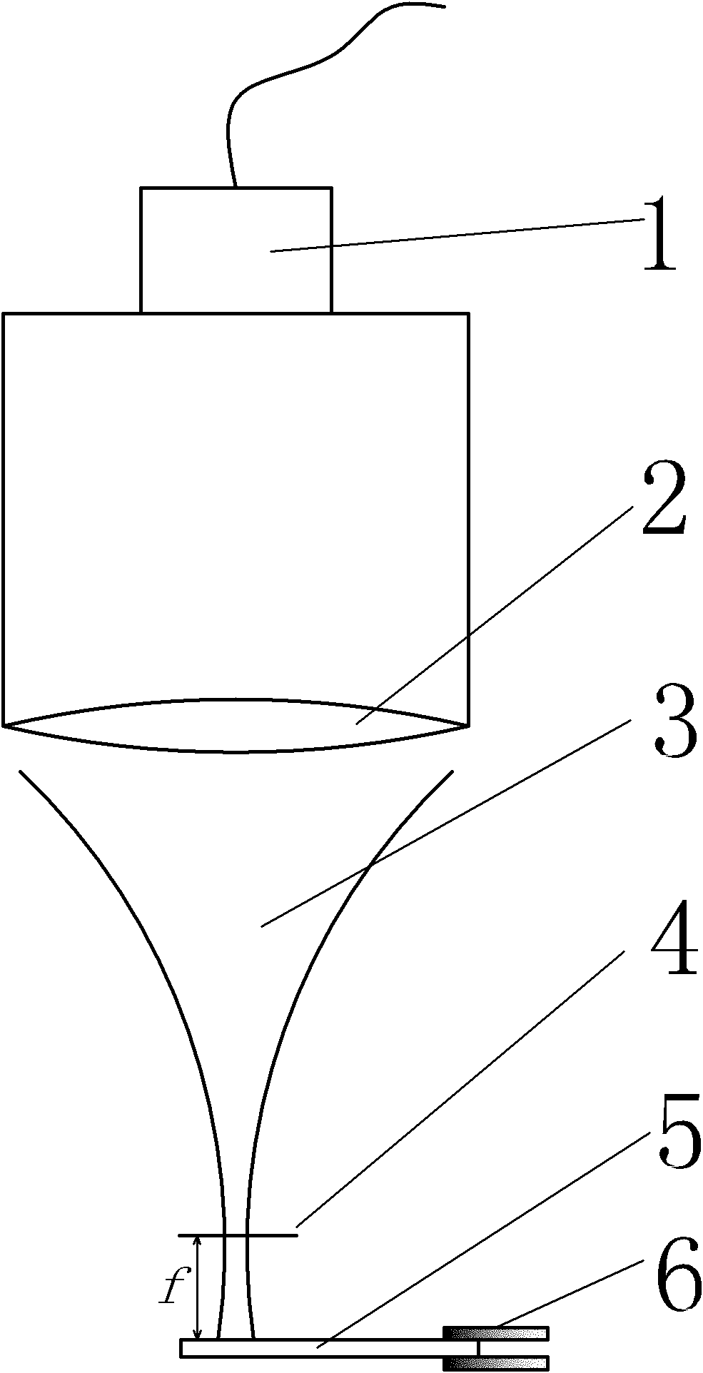
[0024] The present invention will be further described below in conjunction with the drawings. Such as Figure 1-2 As shown, a thin silicon wafer bending forming method uses a laser beam 3 with a wavelength of 1064nm output by a Nd:YAG pulsed laser to scan the silicon wafer, and the thermal action of the laser beam 3 and the thin silicon wafer 5 material is thin silicon The bending of the sheet 5 provides power and temperature conditions, which specifically includes the following steps:

[0025] A. Choose a thin silicon wafer 5 with a scanned length of 2-10mm and a thickness of 0.1-0.3mm, and clean it with deionized water;

[0026] B. Install the thin silicon wafer 5 on the pre-adjusted workbench, and fix one end with the fixing clamp 6; select the pulse width of the Nd:YAG pulse laser between 1 and 10ms, and adjust it through the online video system 1. Focusing lens 2, after determining the focus position 4 of the laser beam, move the focus position 4 of the laser beam so that t...


PUM

PropertyMeasurementUnit
Lengthaaaaaaaaaa
Thicknessaaaaaaaaaa

Abstract

The invention discloses a bending and forming method of a thin silicon wafer, which scans the thin silicon wafer by utilizing Nd:YAG pulse laser and provides power and temperature conditions for bending the thin silicon wafer by thermal action of laser and a thin silicon wafer material. In the bending and forming method, extra temperature environment does not need to be provided in the stage of laser scanning, the bending and forming mainly utilize the thermal action of the laser and the thin silicon wafer material to realize the plastic characteristic of the silicon wafer, and further are realized by stress difference generated by different temperatures on the upper surface and the lower surface. In the bending and forming method, 1064nm pulse laser is utilized to realize bending and forming of the silicon material with the thickness being 0.1mm-0.3mm, a 30-degree bending angle can be obtained, the bending quality is good, simultaneously, the operation is convenient, and the technology is simple, so that the bending and forming method is beneficial to realizing automatization. The laser bending technology adopted by the invention belongs to a non-contact processing form, has no contact damage to the surface of the material, and can effectively avoid damage caused by being contacted with external force in the bending process of the silicon wafer.

Description

Technical field [0001] The invention relates to a manufacturing technology of a semiconductor device, in particular to a bending forming method of a thin silicon wafer. Background technique [0002] With the development of optoelectronic technology, semiconductor devices have not only satisfied the manufacture of planar size, but also increased the demand for complex curved surfaces, especially the application of warped thin silicon beams. Therefore, we are required to use traditional micro-thickness planar structure devices. For further processing. At this time, the thickness of the semiconductor silicon material is relatively thin. If the traditional external force forming is used, it is easy to cause the material to be damaged. Therefore, the external force forming must be carried out under high temperature conditions; while the traditional chemical etching method to achieve bending processing requires a long manufacturing cycle and difficult control It also pollutes the envi...

Claims


Application Information

Patent Timeline
IPC IPC(8): B81C1/00
Inventor 吴东江马广义郭东明刘双
Owner DALIAN UNIV OF TECH
Why Eureka
Try Eureka