Real-time measuring device and method for wave aberration

A technology of real-time measurement and measurement device, which is applied in the direction of photolithography exposure device, test optical performance, micro-lithography exposure equipment, etc., can solve the problems of measurement speed and measurement accuracy, improve accuracy, reduce pulse jitter, The effect of increasing productivity

Active Publication Date: 2011-05-25
SHANGHAI MICRO ELECTRONICS EQUIP (GRP) CO LTD
View PDF3 Cites 27 Cited by
  • Summary
  • Abstract
  • Description
  • Claims
  • Application Information

AI Technical Summary

Problems solved by technology

In this way, the measurement accuracy of wave aberration is limited by the degree of pulse jitter of the light source and the number of received pulses. In the case of constant pulse jitter, the number of received pulses must be increased to improve the measurement accuracy, so the measurement speed is also limited by its measurement Accuracy Constraints

Method used


Image

  • Real-time measuring device and method for wave aberration
  • Real-time measuring device and method for wave aberration
  • Real-time measuring device and method for wave aberration

Examples


Embodiment Construction

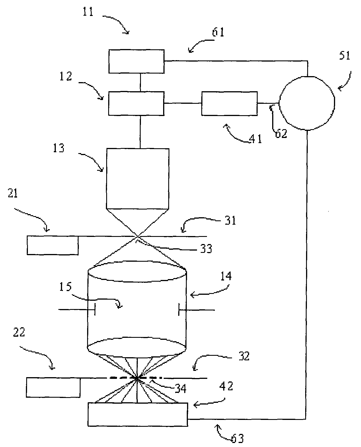
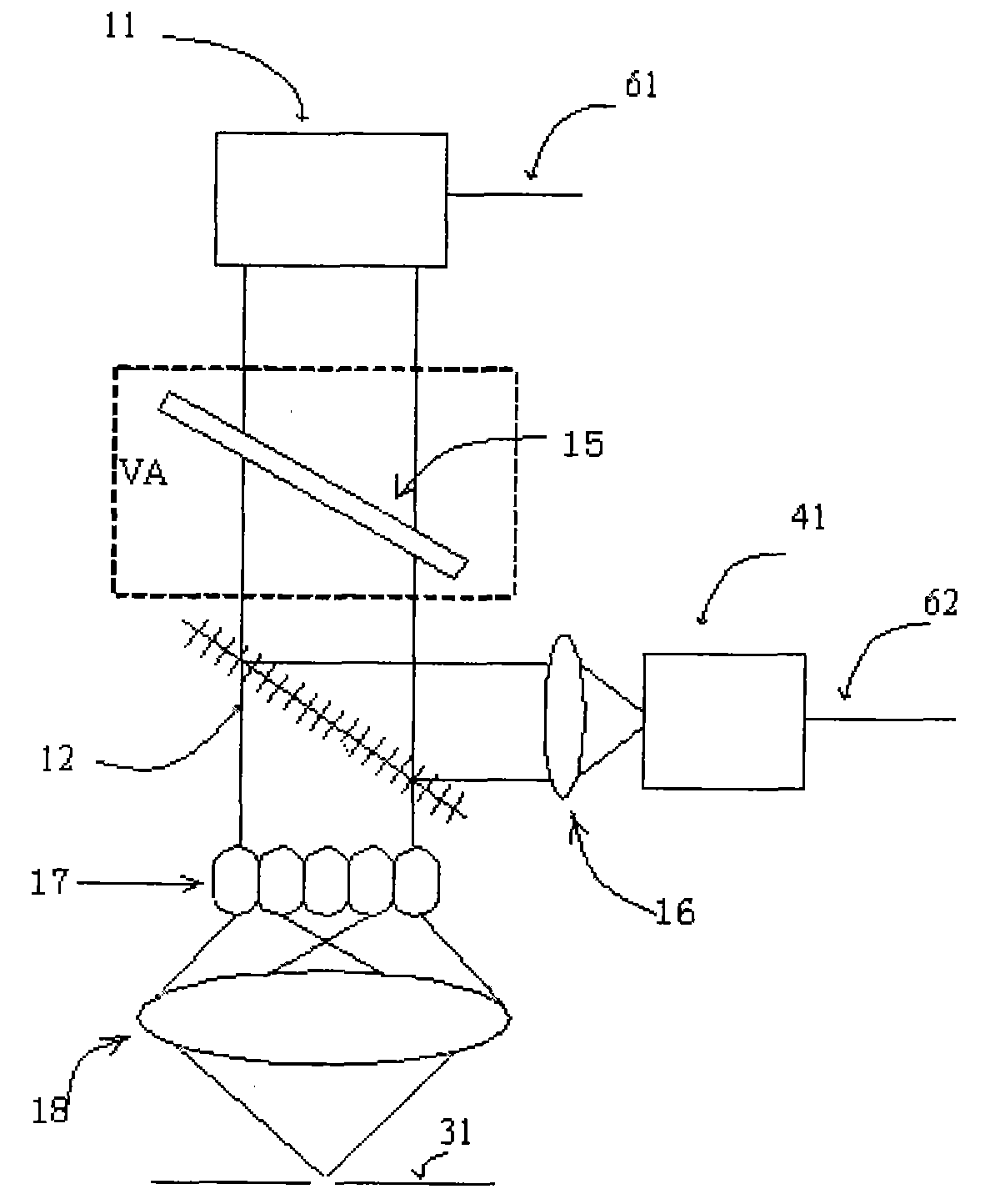
[0038] In the following, preferred embodiments according to the present invention will be described in detail with reference to the accompanying drawings. For the convenience of describing and highlighting the present invention, relevant components existing in the prior art are omitted from the drawings, and the description of these known components will be omitted.

[0039] figure 1 Shown is a schematic diagram of the apparatus used in the present invention. In the figure, 11 is a light source, and 12 is a beam splitter, which splits a part of the light supplied by the light source to the lighting system 13 and is detected by the energy sensor 41 . The aperture 33 produces a probe light source. The small hole is located on the small hole surface 31 . The surface of the small hole coincides with the surface of the object. The small hole surface is connected with the mask table 21 and can move with it. The detection light is diffracted by the shearing grating 34 after pass...


PUM


Abstract

The invention discloses a real-time measuring device for wave aberration, which comprises a light source, a beam splitter, a lighting system, an object surface pinhole, an objective lens system, a shearing grating, a two-dimensional array photosensitive element, an energy sensor, and a synchronous control and comparison part, wherein the beam splitter splits light emitted by the light source into a first light beam and a second light beam; the lighting system receives the first light beam emitted by the beam splitter; the object surface pinhole receives light emitted by the lighting system to form a probe light source; the objective lens system is used for imaging the pinhole; the shearing grating is positioned on the image surface of the objective lens system and diffracts probe light emitted by the pinhole; the probing surface of the two-dimensional array photosensitive element receives shearing interference fringes generated by the shearing grating and is conjugate with the pupilplane of an objective lens; the energy sensor receives the second light beam emitted by the beam splitter; and the synchronous control and comparison part is connected with the light source, the energy sensor and the two-dimensional array photosensitive element through signal wires. During measurement, the synchronous control and comparison part controls the energy sensor and the two-dimensional array photosensitive element to perform synchronous optical energy integral at the same time interval, and a measuring result of the two-dimensional array photosensitive element is calibrated by a measuring result of the energy sensor.

Description

technical field [0001] The invention relates to a device and method for real-time measurement of wave aberration, in particular to a device and method for real-time measurement of wave aberration used in photolithography equipment. Background technique [0002] One goal of the semiconductor industry is to integrate more electronic components into a single integrated circuit (IC). To achieve this goal, the size of the components must be continuously reduced, that is, the resolution of the lithography projection system must be continuously improved. Objective lens wave aberration is an important factor limiting the resolution of a projection system, and it is an important cause of line width variation. [0003] Although the objective lens has been strictly inspected and optimized during the manufacturing and assembly process to minimize its wave aberration, it is still necessary to perform real-time wave aberration measurement after the objective lens system is integrated int...

Claims


Application Information

Patent Timeline
Patent Type & Authority Applications(China)
IPC IPC(8): G03F7/20G01M11/02
Inventor 陆海亮
Owner SHANGHAI MICRO ELECTRONICS EQUIP (GRP) CO LTD
Why Eureka
Try Eureka