High-power semiconductor laser polarization coupling device and coupling method thereof

A coupling device and semiconductor technology, which is applied in the direction of semiconductor laser devices, laser devices, devices for controlling laser output parameters, etc., can solve the problems of output laser brightness and beam quality difficulties, and achieve improved beam quality and optical power density, high brightness and high Effect of Power Laser Output

Inactive Publication Date: 2011-06-01
BEIJING LUHE FEIHONG LASER TECH
View PDF7 Cites 2 Cited by
  • Summary
  • Abstract
  • Description
  • Claims
  • Application Information

AI Technical Summary

Problems solved by technology

At present, the method of collimating the fast and slow axis of the semiconductor laser beam and beam shaping is usually used to improve the beam quality of the output laser of the high-power semiconductor laser, but it is necessary to further compress the size of the input beam of the high-power semiconductor laser and improve the compression of the high-power semiconductor laser. The brightness and beam quality of the output laser are difficult

Method used


Image

  • High-power semiconductor laser polarization coupling device and coupling method thereof
  • High-power semiconductor laser polarization coupling device and coupling method thereof
  • High-power semiconductor laser polarization coupling device and coupling method thereof

Examples


Embodiment 1

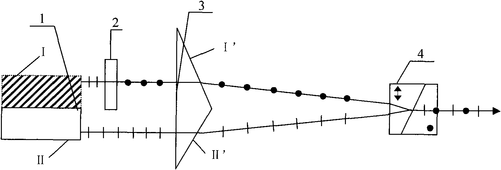
[0024] figure 1 The half-wave plate 2 is placed between the half beam I of the laser light emitted by the semiconductor laser and the side I' of the beam splitting and deflecting prism 3, wherein the lower end of the half-wave plate 2 is placed at the beam splitting deflecting prism. On the central line of the prism 3; half the light beam I of the laser light emitted by the semiconductor laser is p light (polarization direction parallel to the polarized light on the paper) before passing through the half wave plate 2, and after passing through the half wave plate 2 The polarization direction changes by π / 2, and becomes s light (polarized light whose polarization direction is perpendicular to the paper), and half of the laser light beam II emitted by the semiconductor laser is p light. After passing through the deflection prism, a beam of s light and a beam of p light After the light is incident on the Wollaston prism 4, a beam of partially polarized parallel light is synthesiz...

Embodiment 2

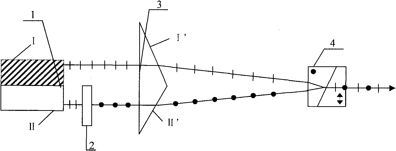
[0026] figure 2 The half-wave plate 2 is placed between the half beam II of the laser light emitted by the semiconductor laser and the side II' of the beam splitting deflection prism 3, wherein the upper end of the half-wave plate 2 is placed at the beam splitting deflection On the central line of the prism 3; half beam I of the laser light emitted by the semiconductor laser is p light, half of the light beam II of the laser light emitted by the semiconductor laser is p light before passing through the half wave plate 2, and passes through the half wave plate After 2, the polarization direction changes by π / 2 to become s light. After passing through the deflection prism, a beam of s light and a beam of p light enter Wollaston prism 4 and then synthesize a beam of partially polarized parallel light to exit, wherein Wollaston The crystal material used in the Raston prism is a negative uniaxial crystal.

Embodiment 3

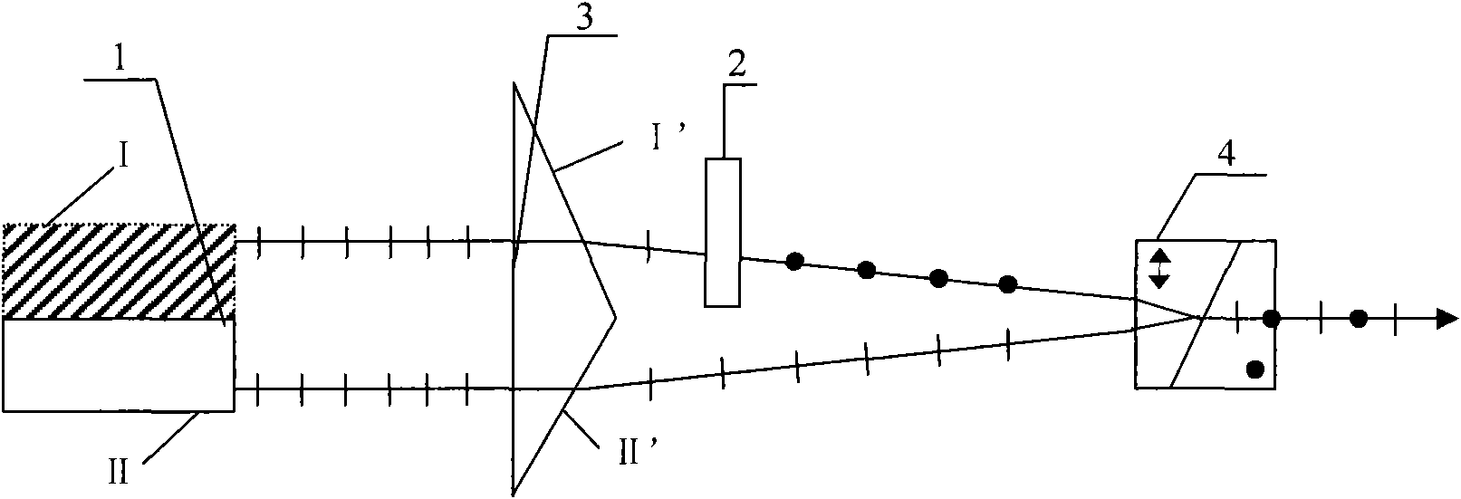
[0028] image 3 For the situation that the half-wave plate 2 is placed between the side I' of the beam splitting deflection prism 3 and the Wollaston prism 4, wherein the lower end of the half wave plate 2 is positioned at the side of the beam splitting deflection prism 3 On the central line, this situation is the same as the principle of embodiment 1;


PUM


Abstract

The invention relates to a semiconductor laser polarization coupling device, belonging to laser photoelectron and the application field thereof. The device comprises a half-wave plate (2), a dispersion deviating prism (3) and a Wollastonprism (4), wherein linear polarized light beams (1) from a semiconductor laser pass through the coupling device; the polarization direction of half of light beams deviates by pi / 2 after passing through the half-wave plate (2); the polarization direction of the other half of the light beams is unchanged; two halves of light beams are deviated and emitted to reach the Wollastonprism (4) through the dispersion deviating prism (3); the light beams continue to deviate; the structure angle of a dispersion prism and the structure angle of the Wollastonprism meet the conditions for emission of parallel rays, light paths are adjusted, and one beam of the partial polarization parallel rays is output, thus realizing size compression of semiconductor laser beams, and improving the beam luminance and the beam quality. According to the invention, high-light and high-beam quality lasers with the order of magnitude of over kilowatt can be output. The coupling device is simple in structure, easy to realize and low in cost, and can meet different application requirements.

Description

technical field [0001] The invention is a device for polarizing and coupling the output beam of a high-power semiconductor laser through a beam splitting deflection prism and a Wollaston prism to improve the brightness and quality of the output beam, and belongs to the field of laser optoelectronics and its application. Background technique [0002] Semiconductor lasers are widely used in various fields due to their small size, high photoelectric conversion rate and long life. In particular, kilowatt-level high-power semiconductor lasers with high beam quality and high brightness have a wide range of applications and great development prospects in material processing, pumping solid-state lasers, and in military and medical fields. Therefore, how to realize a kilowatt-class high-power semiconductor laser with high beam quality and high brightness has become a hot issue. Semiconductor laser arrays (including one-dimensional semiconductor laser arrays and two-dimensional semic...

Claims


Application Information

Patent Timeline
Patent Type & Authority Applications(China)
IPC IPC(8): H01S5/40H01S5/06G02B27/09G02B27/28
Inventor 王智勇高静曹银花刘友强
Owner BEIJING LUHE FEIHONG LASER TECH
Why Eureka
Try Eureka