Corrosive solution composition, corrosion method and generated silicon wafer

A technology for etching solutions and compositions, applied in the manufacture of electrical components, circuits, semiconductor/solid-state devices, etc., can solve problems such as affecting product quality, blackening and dyeing, and achieve the effect of maintaining stable corrosion rate and improving quality

Active Publication Date: 2012-10-10
FOUNDER MICROELECTRONICS INT
View PDF0 Cites 0 Cited by
  • Summary
  • Abstract
  • Description
  • Claims
  • Application Information

AI Technical Summary

Problems solved by technology

[0003] At present, the etching process used in the backside silicon etching process in the industry makes the backside of the wafer often appear blackened and stained after the process is completed, that is, a silicon dioxide layer is formed on the etched surface of the wafer after silicon etching, which affects the quality of the product.

Method used


Image

  • Corrosive solution composition, corrosion method and generated silicon wafer

Examples


Embodiment Construction

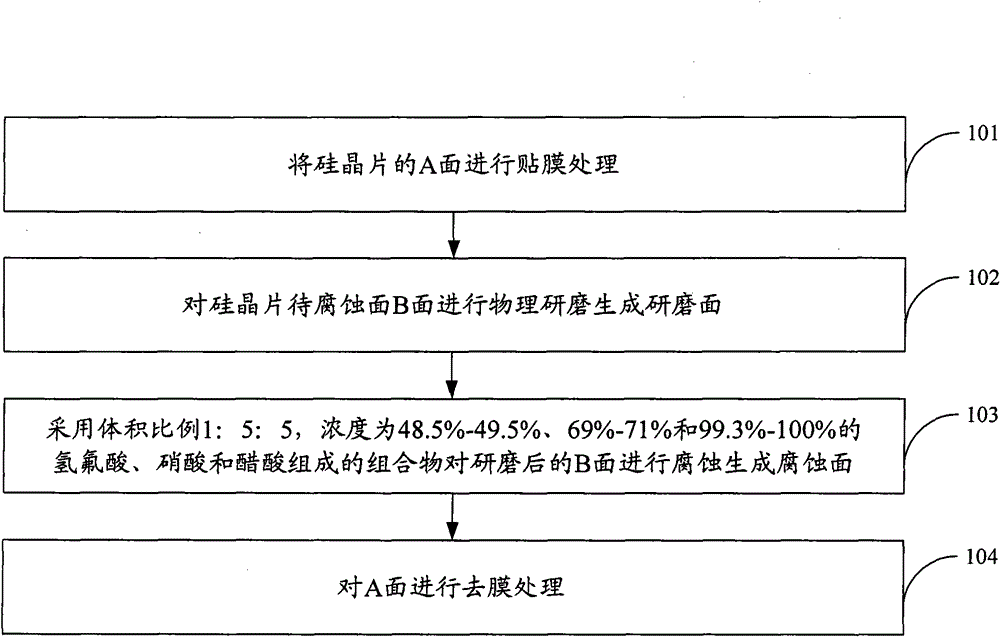
[0011] In order to solve the problem in the prior art that a silicon dioxide layer is formed on the corroded surface of the wafer after silicon corroding, which affects the quality of the product, an embodiment of the present invention provides a composition of etching solution, which is composed of hydrofluoric acid, nitric acid and acetic acid composition. Among them, the concentration of hydrofluoric acid is 48.5%-49.5%, the concentration of nitric acid is 69%-71%, and the concentration of acetic acid is 99.3%-100%. Of course, acetic acid CH3COOH is only a preferred solution in this embodiment, and other weak acids such as carbonic acid H2CO3, boric acid H3BO3 and weakly acidic organic acids can also be used. A preferred solution in this embodiment is that the volume ratio of hydrofluoric acid, nitric acid and acetic acid is 1:5:5, and the surface to be etched of the silicon crystal is etched, and the specific reaction process is as follows:

[0012] Si+4HNO 3 → SiO 2 +2...


PUM


Abstract

The invention discloses a corrosive solution composition, a corrosion method and a generated silicon wafer in order to solve the problem in the prior art that the product quality is influenced as a silicon dioxide layer is generated on the corroded surface of the corroded silicon wafer. The method disclosed by the invention comprises the following steps: physically grinding the surface to be corroded of the silicon wafer; and corroding the ground surface with a composition consisting of 48.5-49.5% hydrofluoric acid, 69-71% nitric acid and 99.3-100% acetic acid in a volume proportion of 1:5:5 so as to generate the corroded surface. As the ground surface is corroded by the composition, a silicon dioxide layer is prevented from being generated on the corroded surface, and the quality of the silicon wafer is improved.

Description

technical field [0001] The invention belongs to the technical field of semiconductor device production, and in particular relates to an etching solution composition, an etching method and a produced silicon wafer. Background technique [0002] In today's integrated circuits, the backside silicon etching process is used in the backside process of discrete devices. The specific process flow is as follows. Since the backside is thinned by physical grinding, the stress on the backside after thinning is relatively large, and the warpage is serious. For the risk of fragmentation, increasing the silicon etching process on the back side after thinning can eliminate the stress after thinning, so that the flatness of the wafer can meet the requirements, greatly reducing the risk of fragmentation, and improving the online survival rate of products. [0003] At present, the etching process used in the backside silicon etching process in the industry makes the backside of the wafer often...

Claims


Application Information

Patent Timeline
Patent Type & Authority Patents(China)
IPC IPC(8): H01L21/306
Inventor 林国胜
Owner FOUNDER MICROELECTRONICS INT
Why Eureka
Try Eureka