Two-dimensional photonic crystal T-shaped waveguide based on surface state of photonic crystals

A two-dimensional photonic crystal and photonic crystal technology, applied in light guides, optics, optical components, etc., can solve the problems of large reflection, large waveguide area, low transmission efficiency, etc., and achieve the effect of zero reflection

Active Publication Date: 2011-06-08
INST OF SEMICONDUCTORS - CHINESE ACAD OF SCI
View PDF4 Cites 13 Cited by
  • Summary
  • Abstract
  • Description
  • Claims
  • Application Information

AI Technical Summary

Problems solved by technology

[0007] In view of this, the main purpose of the present invention is to provide a two-dimensional photonic crystal T-shaped waveguide based on the surface state of photonic crystals, to overcome the problems of large area, low transmission efficiency and large reflection of traditional waveguides.

Method used


Image

  • Two-dimensional photonic crystal T-shaped waveguide based on surface state of photonic crystals
  • Two-dimensional photonic crystal T-shaped waveguide based on surface state of photonic crystals
  • Two-dimensional photonic crystal T-shaped waveguide based on surface state of photonic crystals

Examples


Embodiment 1

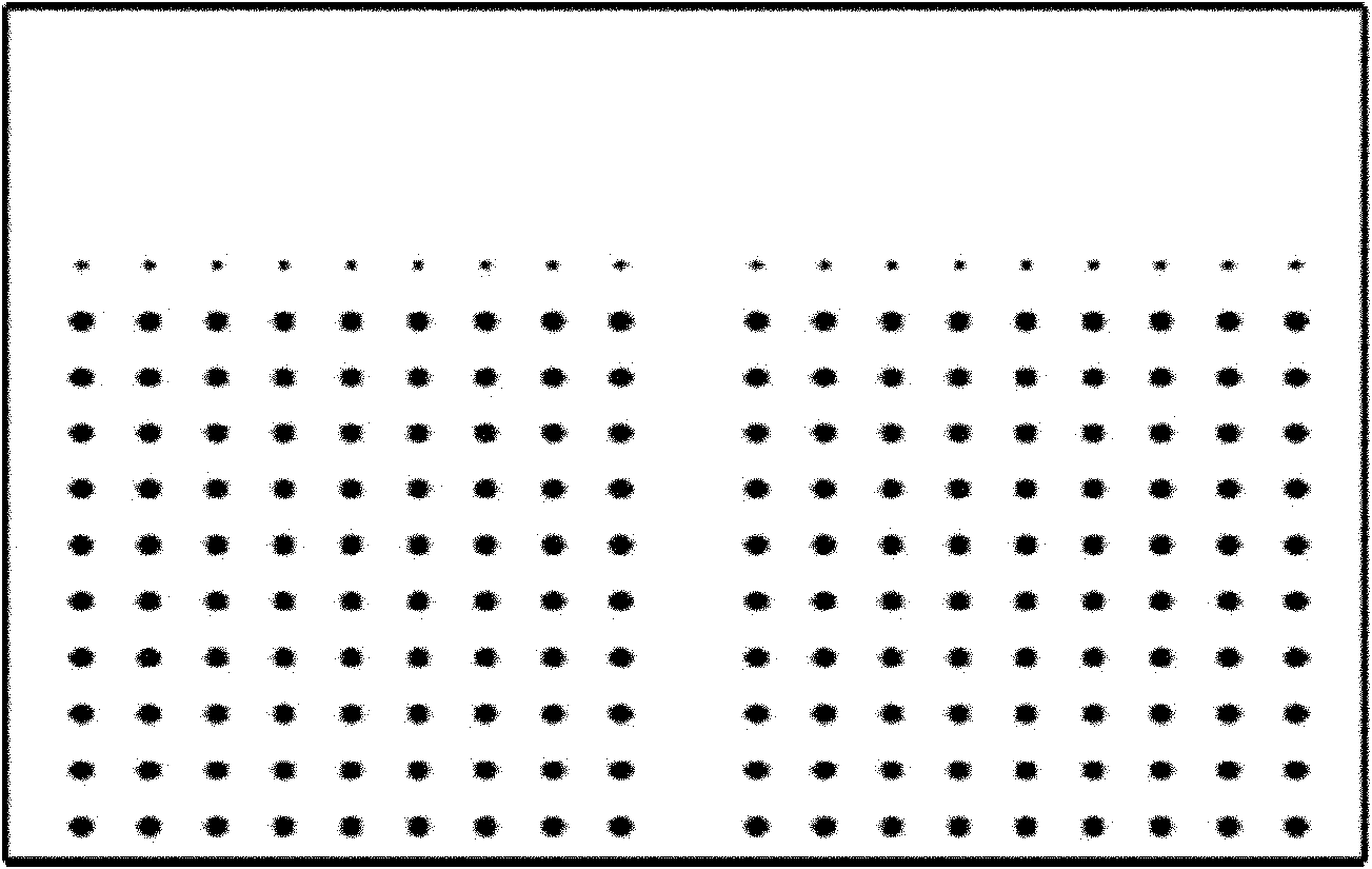
[0039] figure 1 A simple, unadjusted two-dimensional photonic crystal T-shaped waveguide based on photonic crystal surface states is provided for the present invention. The parameters used are as follows:

[0040] The dielectric coefficient ε=11.56.

[0041] The radius of the periodic dielectric column is r=0.18a (a is the lattice constant).

[0042] The radius of a row of defective dielectric columns at the exit end of the T-shaped waveguide is r=0.09a.

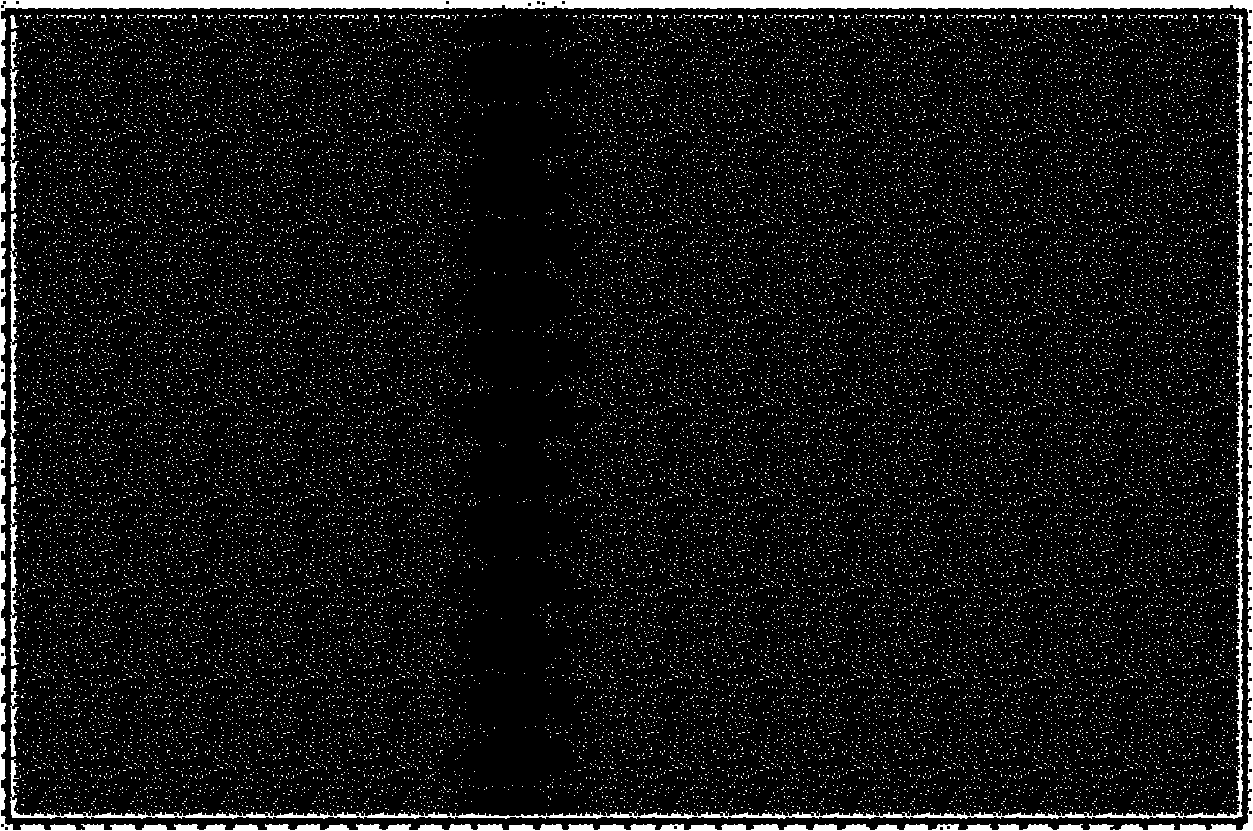
[0043] Figure 5 For light with a wavelength of 1.55 μm at figure 1 Propagated in the structure, the mode field distribution map after stabilization. It can be seen that due to the introduction of the surface mode, part of the energy is transmitted along the left and right branches of the T-shaped waveguide, but it can be clearly seen that the energy intensity transmitted to the two sides is relatively small. Moreover, it can also be seen that part of the energy is directly transmitted into the air along the W1 wavegui...

Embodiment 2

[0046] Figure 7 The fine-tuned two-dimensional photonic crystal T-type waveguide based on the photonic crystal surface state provided by the present invention. The parameters used are as follows:

[0047] The dielectric coefficient ε=11.56.

[0048] The radius of the periodic dielectric column is r=0.18a (a is the lattice constant).

[0049] The radius r=0.09a of a row of defective dielectric pillars on the surface of the photonic crystal on both sides of the T-shaped waveguide exit.

[0050] The radius of the two rows of dielectric columns outside the exit end of the W1 waveguide is r=0.18a.

[0051] The radius of the nearest row of dielectric columns near the exit end of the W1 waveguide is r=0.09a.

[0052] Figure 8 For light with a wavelength of 1.55 μm at Figure 7 Propagated in the structure, the mode field distribution map after stabilization. In the improved T-shaped waveguide, it can be seen that due to the introduction of the surface mode, most of the energy...


PUM


Abstract

The invention discloses a two-dimensional photonic crystal T-shaped waveguide based on a surface state of photonic crystals. The two-dimensional photonic crystal T-shaped waveguide comprises a square lattice photonic crystal W1 waveguide, wherein a row of defect-layer square lattice photonic crystal dielectric cylinders are arranged on photonic crystal surfaces at both sides of the outlet end of the photonic crystal W1 waveguide; multiple rows of reflective square lattice photonic crystal dielectric cylinders are arranged on the outer side of the outlet end of the photonic crystal W1 waveguide; and the row of square lattice photonic crystal dielectric cylinders most close to the outlet end of the photonic crystal W1 waveguide can be used for adjusting the optical field distribution together with the reflective square lattice photonic crystal dielectric cylinders by finely adjusting the size of the square lattice photonic crystal dielectric cylinders. According to the invention, a high-efficiency waveguide, which has an area about half of that of the conventional T-shaped waveguide and has a high transmission rate (up to 90.9%), can be designed. Compared to the conventional T-shaped waveguide, the two-dimensional photonic crystal T-shaped waveguide based on the surface state of the photonic crystals also has the advantage that the reflectivity of the incident end can be a very small number which is almost 0.

Description

technical field [0001] The invention relates to the technical field of semiconductor optoelectronic devices, in particular to a two-dimensional photonic crystal T-shaped waveguide based on photonic crystal surface states. Background technique [0002] Photonic crystals have the characteristics of photon bandgap, suppression of spontaneous emission of atoms and molecules, etc. In the past 20 years, they have aroused people's wide interest and been extensively studied all over the world. Theoretical and experimental studies have shown that the introduction of defects in photonic crystals can introduce defect states in the photonic band gap, realize the localization of light, enhance the interaction between light and matter, and provide photonic crystals with low threshold or even no threshold lasers. , waveguide and other aspects of the application provides a broad prospect, but also laid a solid foundation for the realization of high-density optical integration, high-efficien...

Claims


Application Information

Patent Timeline
Patent Type & Authority Applications(China)
IPC IPC(8): G02B6/122
Inventor 江斌刘安金陈微周文君郑婉华
Owner INST OF SEMICONDUCTORS - CHINESE ACAD OF SCI
Why Eureka
Try Eureka