Semiconductor memory device

Inactive Publication Date: 2011-09-29
HITACHI LTD
View PDF13 Cites 58 Cited by
  • Summary
  • Abstract
  • Description
  • Claims
  • Application Information

AI Technical Summary

Benefits of technology

[0027]According to the invention, it is possible to decrease the write current or

Problems solved by technology

Accordingly, the data transfer rate in a solid memory using the phase-change material is limited by a permissible combustion power.
For the improvement, when the technique of the heater layer described in JP-A-2009-117854 is introduce

Method used


Image

  • Semiconductor memory device
  • Semiconductor memory device
  • Semiconductor memory device

Examples


Example

Example 1

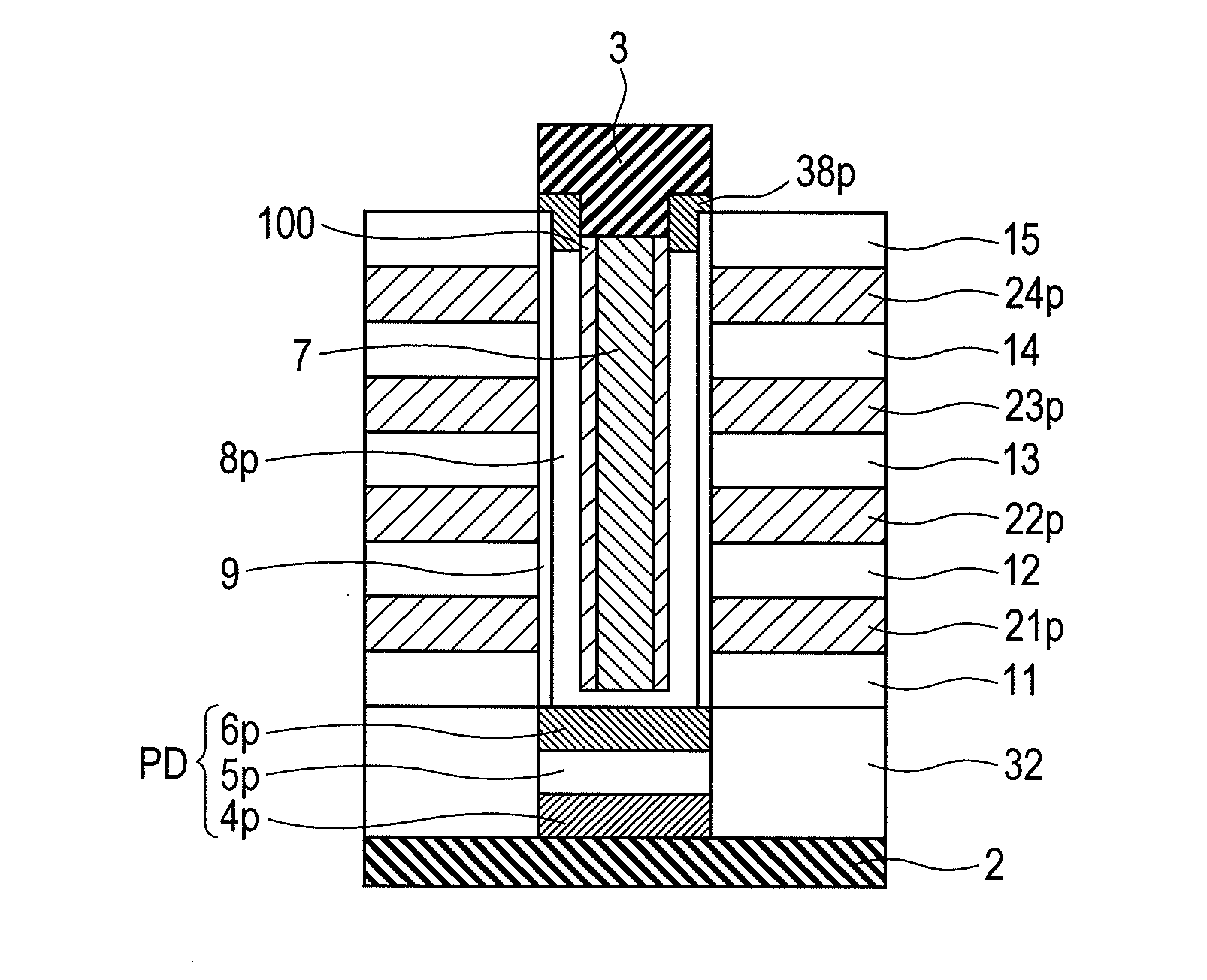
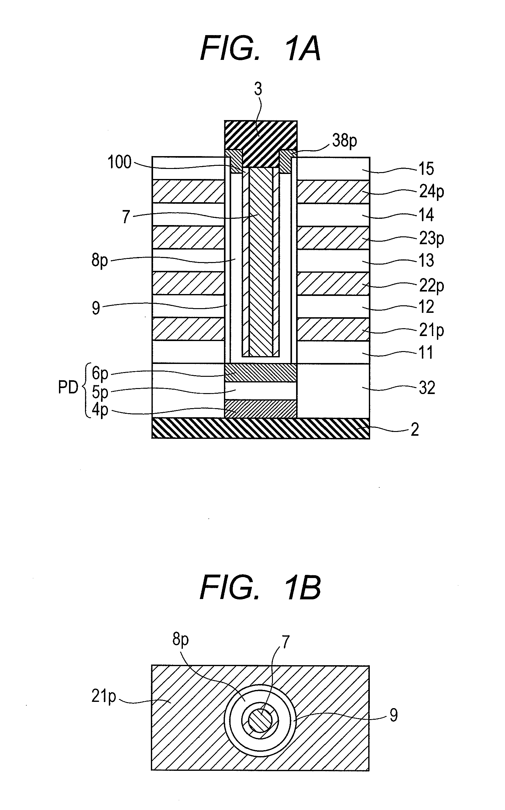
[0070]FIGS. 1A and 1B show an example of a model of a phase-change memory having a vertical memory structure. FIG. 1A is a cross sectional view in the vertical direction and FIG. 1B is a cross sectional view in a horizontal direction for a portion shown by a reference 21p. The drawing shows a phase-change memory material (phase-change-material layer) 7, an interface layer 100, and a channel polysilicon layer (channel layer) 8p for flowing a write current. Further, gate polysilicon layers (gate layers) 21p, 22p, 23p, and 24p, and insulating film layers (inter-gate-layer insulating films) 11, 12, 13, 14, and 15 are formed alternately, and a channel polysilicon layer 8p, and a phase-change layer are disposed continuously on the lateral sides thereof. That is, the stack has a connection hole that connects the upper surface and the lower surface of the gate polysilicon layers 21p, 22p, 23p and 24p, and the insulating film layers 11, 12, 13, 14, and 15 formed alternately, and the...

Example

Example 2

[0109]As described above, at the minimum feature size of 32 nm by lithography, the film thickness of the phase-change material was about 4 nm. For proceeding the refinement further, it is necessary for the phase-change material to conduct reversible switching between amorphous and crystalline states at the film thickness of less than 4 nm. It has been generally considered that crystallization becomes difficult and switching operation is no more shown when the thickness of the phase-change material is about 6 nm or less. Then, by utilizing the resistance measurement device described above, the film thickness and the switching characteristics of the phase-change material sandwitched by various interface material films were measured. In this example, a Ge2Sb2Te5 compound material was used as the phase-change material. FIG. 30 to FIG. 32 show the result of measuring the resistivity change from an as deposited amorphous state to a crystalline state in the same manner as describe...

Example

Example 3

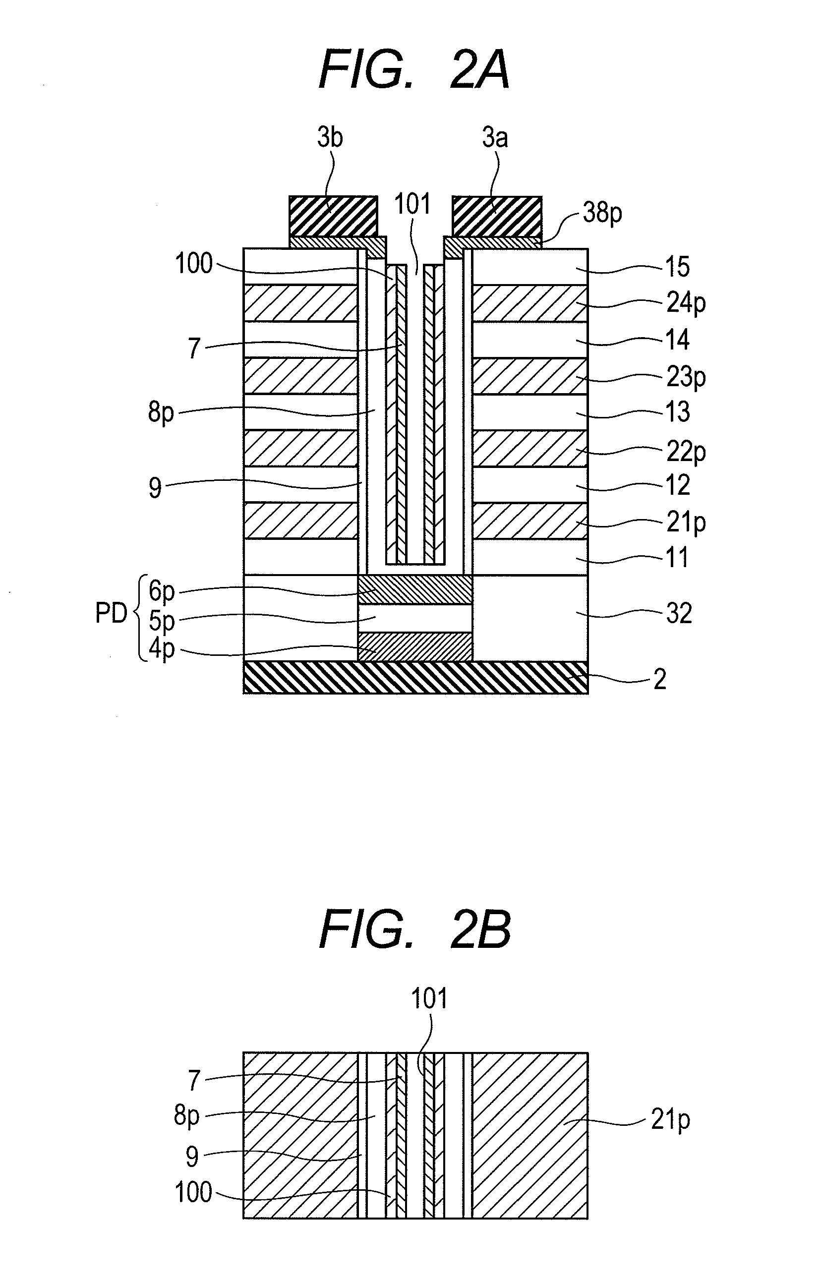
[0129]Then, description is to be made to a recording method of suppressing cross-erase as a second object of the invention. FIG. 36A is a schematic view for the structure shown in FIG. 2A. GP corresponds to a gate poly silicon layer, which is isolated by an insulating film INS. Further, a member X is formed on the side wall of the gate polysilicon layer GP and the insulating film INS in which gate insulating film-channel portion (polysilicon channel)-phase-change material layer-insulating film-phase-change material layer-channel portion (polysilicon channel)-gate insulating film are disposed from the left. For the sake of simplicity of the description, thin interface layer thin film shown in FIG. 2 is not illustrated. In the invention described in Example 3, the interface layer film may or may not be present.

[0130]Then, as the lateral refinement is proceeded, since the aspect ratio becomes greater, the size in the vertical direction is also decreased. Then, a gap between th...


PUM


Abstract

For decreasing a recording current and suppressing a cross erase simultaneously, a three-dimensional phase-change memory for attaining higher sensitivity and higher reliability by the provision of a chalcogenide type interface layer is provided, in which an electric resistivity, a thermal conductivity, and a melting point of the material of the interface layer are selected appropriately, thereby improving the current concentration to the phase-change material and thermal and material insulation property with Si channel upon writing.

Description

CLAIM OF PRIORITY[0001]The present application claims priority from Japanese patent application JP 2010-067204 filed on Mar. 24, 2010, the content of which is hereby incorporated by reference into this application.FIELD OF THE INVENTION[0002]The present invention concerns a solid memory device and a recording method thereof and it particularly relates to a semiconductor memory device capable of rewriting for storing information by utilizing a material whose electric resistance changes reversibly by flowing a current to the device.BACKGROUND OF THE INVENTION[0003]In recent years, resistance change type memories have been studied as a substitute for flash memories which are now approaching the limit of refinement and, as an example, phase-change memories have been studied vigorously using chalcogenide materials as the recording material. In a basic structure of the phase-change memory, a recording material is put between metal electrodes. The phase-change memory is a resistance, chang...

Claims


Application Information

Patent Timeline
IPC IPC(8): G11C11/00H01L47/00
CPCH01L27/2409H01L27/2454H01L27/2481H01L45/06H01L45/1233H01L45/1286G11C2213/75H01L45/144G11C13/0004G11C13/0069G11C2013/008G11C2213/71H01L45/1293H10B63/34H10B63/20H10B63/84H10N70/231H10N70/8616H10N70/826H10N70/8613H10N70/8828
Inventor MINEMURA, HIROYUKIANZAI, YUMIKOMORIKAWA, TAKAHIROSHINTANI, TOSHIMICHISASAGO, YOSHITAKA
Owner HITACHI LTD
Why Eureka
Try Eureka