Device and method for nanoimprinting of full wafer

A nano-imprinting and wafer technology, which is applied in the photoplate process, instrument, optics and other directions of the pattern surface, and can solve the problem of small imprinting force and excessive demoulding force, uneven wafer, dirt on the wafer, etc. problems, to achieve the effect of eliminating air bubbles, ensuring the accuracy of the complex, and achieving uniform distribution

Active Publication Date: 2012-04-04
QINGDAO TECHNOLOGICAL UNIVERSITY
View PDF0 Cites 5 Cited by
  • Summary
  • Abstract
  • Description
  • Claims
  • Application Information

AI Technical Summary

Problems solved by technology

[0003] The present invention is aimed at the nanoimprinting of the whole wafer and faces: uniform imprinting force over a large area, requiring as little imprinting force and demoulding force as possible, bubble elimination, uniform and thin residual layer thickness, and effective large area Challenging issues such as the release method, for the imprinting of LED epitaxial wafers, the wafer is uneven, the wafer has dirt, and the substrate material is brittle and fragile.

Method used


Image

  • Device and method for nanoimprinting of full wafer
  • Device and method for nanoimprinting of full wafer
  • Device and method for nanoimprinting of full wafer

Examples


Embodiment Construction

[0043] The present invention will be described in further detail below in conjunction with the accompanying drawings and embodiments.

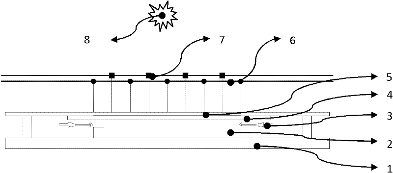
[0044] figure 1 Among them, it includes: a workbench 1, a whole wafer coated with resist 2, a nozzle for demoulding 3, a template 4, an embossing head 5, a pressure pipeline 6, a vacuum pipeline 7 and an ultraviolet light source 8 ; Wherein, the template 4 is fixed on the bottom surface of the embossing head 5, and the lower side of the template 4 is provided with a nozzle 3 for demoulding; the pressure pipeline 6 and the vacuum pipeline 7 are connected to the air inlets on both sides of the embossing head worktable; The entire wafer 2 covered with resist is fixed on the wafer workbench 1 ; the ultraviolet light source 8 is placed on the imprint head 5 .

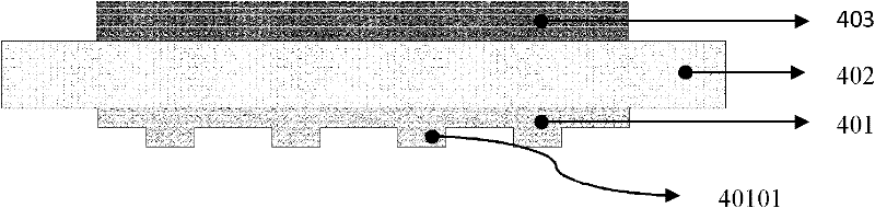
[0045] figure 2 Among them, the template 4 is a transparent flexible mold with a three-layer composite structure, wherein the first layer (lowest layer) is a structural layer 401, the sec...


PUM

PropertyMeasurementUnit
thicknessaaaaaaaaaa
thicknessaaaaaaaaaa
depthaaaaaaaaaa

Abstract

The invention relates to a device and a method for nanoimprinting of a full wafer, comprising a working platform, a full wafer coated with an etchant resist, a nozzle for demoulding, a template, an imprinting head, a pressure pipeline, a vacuum pipeline and an ultraviolet light source, wherein the template is fixed on the bottom surface of the imprinting head; the side surface on the lower part of the template is equipped with the nozzle for demoulding; the pressure pipeline and the vacuum pipeline are connected to air inlet holes which are arranged on two side surfaces of the working platform of the imprinting head; the full wafer coated with the etchant resist is fixed on a wafer working platform; and the ultraviolet light source is arranged over the imprinting head. The method providedby the invention comprises the following steps of: 1) pre-treating process; 2) imprinting process; 3) curing process; and 4) demoulding process. The device and the method for nanoimprinting of the full wafer provided by the invention have the characteristics that the structure is simple, the cost is low, the production efficiency is high, the accuracy is high, the imprinting area is large, and the suitability for the batch production and the imprinting of the full uneven wafer can be obtained. The device and the method can be applied to the large-scale manufacturing of high-density disc, micro-optic device and micro-fluidic device and the like, and the device and the method are particularly suitable for the imaging of the full wafer of a photonic crystal LED (Light Emitting Diode).

Description

technical field [0001] The invention relates to a device and method for nano-imprinting of a whole wafer to realize patterning of a whole wafer of a photonic crystal LED, and belongs to the technical field of micro-nano manufacturing and optoelectronic device manufacturing. Background technique [0002] Nanoimprint lithography (Nanoimprint Lithography, NIL) is a new micro-nano patterning method, which is a technology that uses a mold to realize its patterning through the force deformation of the resist. Compared with other micro-nano manufacturing methods, NIL has the characteristics of high resolution, ultra-low cost (NIL at the same production level assessed by international authoritative organizations is at least an order of magnitude lower than traditional optical projection lithography) and high productivity, especially in large-area micro-nano It has outstanding advantages in the manufacture of nanostructures and complex three-dimensional micro-nanostructures. With th...

Claims


Application Information

Patent Timeline
Patent Type & Authority Patents(China)
IPC IPC(8): G03F7/00
Inventor 兰红波丁玉成
Owner QINGDAO TECHNOLOGICAL UNIVERSITY
Why Eureka
Try Eureka