Trench metal-oxide semiconductor field effect transistor (MOSFET) and manufacture method thereof

A technology of oxide semiconductors and field effect transistors, applied in semiconductor/solid-state device manufacturing, semiconductor devices, transistors, etc., can solve the problems of reduced contact area, poor contact characteristics, and reduced avalanche breakdown characteristics of devices Effect of small device size and reduced resistance

Inactive Publication Date: 2011-06-15
FORCE MOS TECH CO LTD
View PDF0 Cites 7 Cited by
  • Summary
  • Abstract
  • Description
  • Claims
  • Application Information

AI Technical Summary

Problems solved by technology

However, with the further reduction in the size of trench metal-oxide-semiconductor field-effect transistor devices, figure 1 The contact area between the P+ contact region 116 and the source metal 120 of the structure shown in is also r

Method used


Image

  • Trench metal-oxide semiconductor field effect transistor (MOSFET) and manufacture method thereof
  • Trench metal-oxide semiconductor field effect transistor (MOSFET) and manufacture method thereof
  • Trench metal-oxide semiconductor field effect transistor (MOSFET) and manufacture method thereof

Examples


Embodiment Construction

[0063] The invention will be described in detail below with reference to the accompanying drawings, in which preferred embodiments of the invention are shown. The invention can, however, be embodied in different ways and should not be limited to the embodiments described herein. For example, the description here refers more to N-channel trench MOSFETs, but clearly other devices are possible.

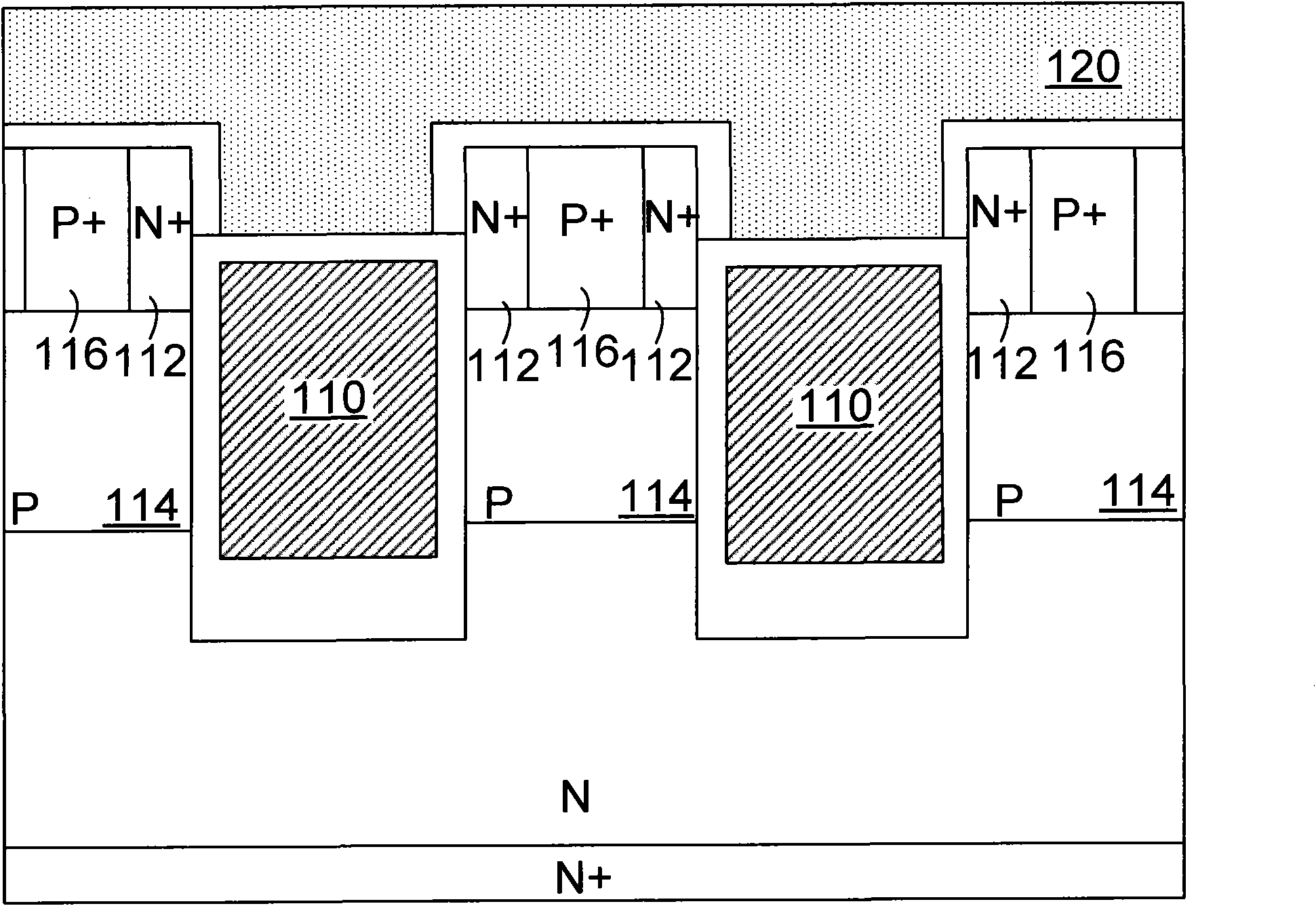
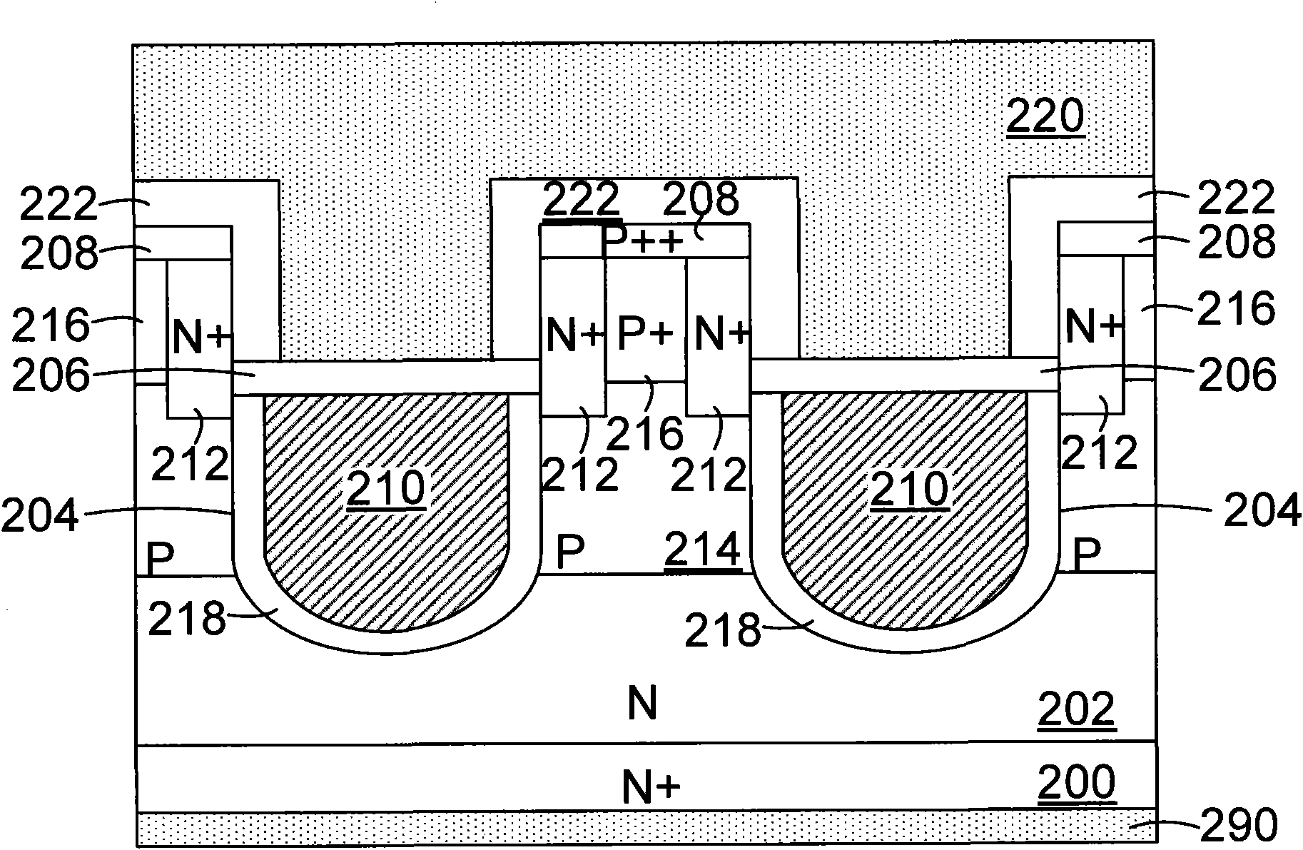
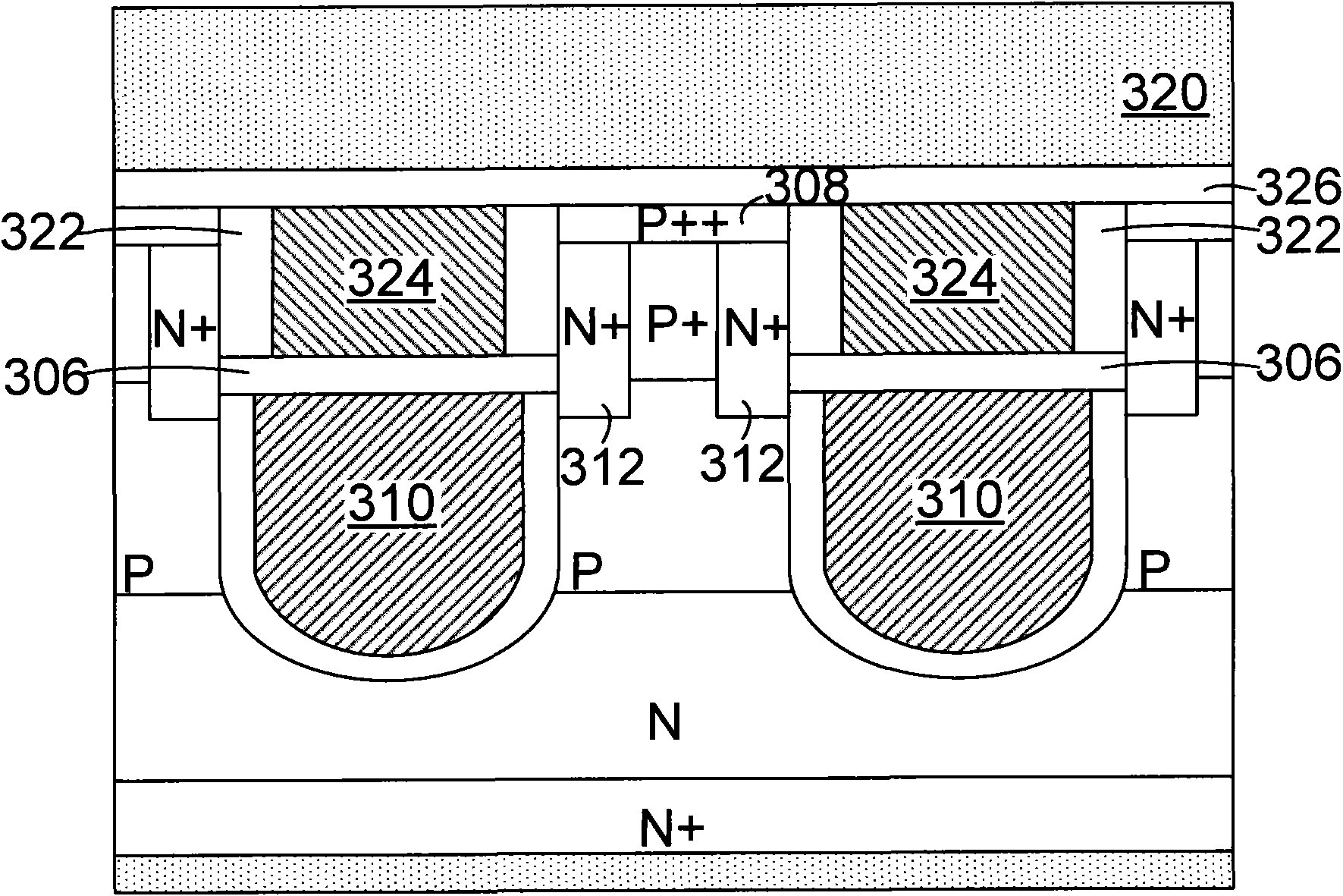
[0064] refer to figure 2 A preferred embodiment of the invention is shown. The N-channel trench MOSFET according to this preferred embodiment is formed on an N+ substrate 200, and the lower surface of the substrate is deposited with a drain metal 290, which is preferably Ti / Ni / Ag. The N-type epitaxial layer 202 is formed on the upper surface of the substrate 200 and has a lower majority carrier concentration than the substrate. A plurality of trenches 204 are formed in the epitaxial layer 202 and are lined with a gate oxide layer 218 between the trenches 204 and the doped polysilicon...


PUM


Abstract

The invention discloses a trench metal-oxide semiconductor field effect transistor (MOSFET) and a manufacture method thereof. A heavily doped contact region is arranged at the top of a table between two adjacent trench grids in an epitaxial layer in the structure. The trench MOSFET provided by the invention can be used for effectively avoiding the problem of drop of the avalanche breakdown characteristic while improving the unit density of the device.

Description

technical field [0001] The invention relates to a unit structure, device structure and process manufacturing of a semiconductor power device, in particular to a unit structure and a process method of a trench MOSFET (Metal Oxide Semiconductor Field Effect Transistor). Background technique [0002] In order to increase the cell density of trench metal oxide semiconductor field effect transistors (MOSFET), the prior art discloses various structures for reducing the mesa width between trench gates, a typical structure such as figure 1 shown. The trench MOSFET includes: an N+ source region 112 formed above the P-type body region 114; a plurality of trench gates 110 located in the active region surrounded by the N+ source region 112; located between adjacent N+ source regions 112 inside the mesa The P+ contact region 116; the source metal 120 in contact with the N+ source region 112 and the P-type body region 114. In addition, the source metal 120 extends into the trench to for...

Claims


Application Information

Patent Timeline
IPC IPC(8): H01L27/088H01L29/78H01L29/06H01L29/36H01L21/8234H01L21/336
Inventor 谢福渊
Owner FORCE MOS TECH CO LTD
Why Eureka
Try Eureka