
Magnetoresistance device

A magnetoresistive device, the technology of the device, applied in the fields of magnetic field controlled resistors, instruments, magnetic recording, etc., can solve the problems of reducing the output signal, reducing the magnetic field strength, increasing the separation, etc.

Inactive Publication Date: 2013-10-23
HITACHI LTD
View PDF7 Cites 0 Cited by
  • Summary
  • Abstract
  • Description
  • Claims
  • Application Information

AI Technical Summary

Problems solved by technology

[0011] The disadvantage of this device is that it requires a thick (about 75nm) passivation layer to protect and confine the active layer and an insulating coating in the form of silicon nitride
This increases the separation between the channel and the magnetic medium, and thereby reduces the magnetic field strength, thereby reducing the output signal

Method used


Image

  • Magnetoresistance device
  • Magnetoresistance device
  • Magnetoresistance device

Examples


Embodiment Construction

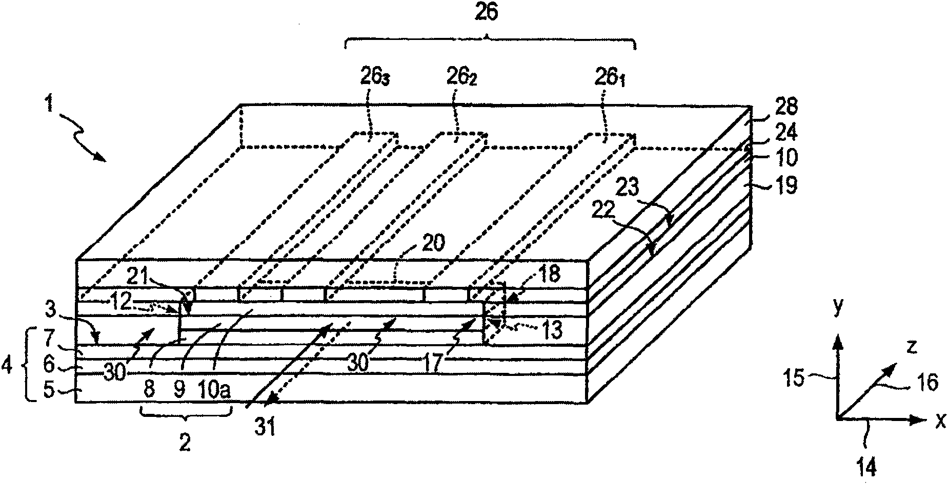
[0077] First magnetoresistive device 1

[0078] Device structure

[0079] refer to figure 1 , 1a , 1b, 2 and 3, show the first magnetoresistive device 1.

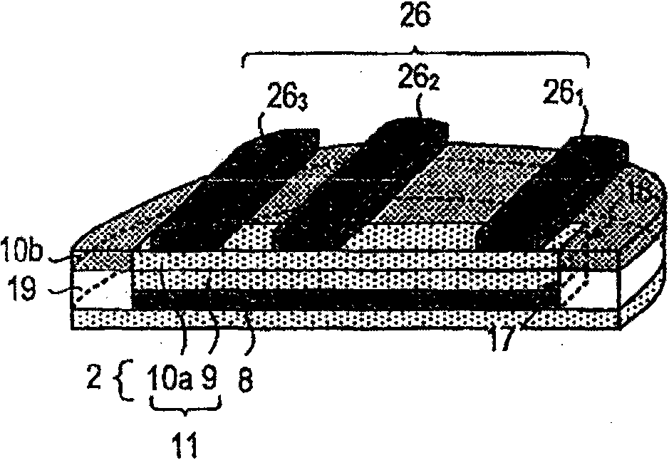
[0080] The component 1 comprises a layer structure 2 arranged on a surface 3 of a generally planar substrate 4 . The substrate 4 takes the form of a semiconductor-on-insulator substrate, which includes a semiconductor base 5 (hereinafter referred to as a "handle layer"), an insulating buried layer 6, and a layer having a thickness t 1 semiconductor top layer 7 . As will be described in detail below, the semiconductor surface layer 7 uses a seed layer for the subsequent epitaxial growth of the layers 8, 9, 10a. The semiconductor substrate 5 and the insulating buried layer 6 may be sacrificial layers. Another substrate 64 ( Figure 19 ) can be connected to face 65 on the opposite side of the remainder of the device ( Figure 19 ).

[0081] In this example, a silicon-on-insulator substrate 4 is used. Thus, the semi...


PUM


Abstract

A magnetoresistance device comprises a substrate (4; 64), an elongate semiconductor channel (11) extending in a first direction (14) and at least two conductive leads (26) providing a set of contacts (27) to the channel. The device may comprise an optional semiconductor shunt (8) in contact with the channel. The optional shunt, channel and set of contacts are stacked relative to the substrate in a second direction (15) which is perpendicular to the first direction and the surface of the substrate. The device has a side face (30) running along the channel. The device is responsive to a magnetic field (31) generally perpendicular to the side face.

Description

technical field [0001] The present invention relates to magnetoresistive devices particularly, but not exclusively, for use as read heads in hard disk drives. Background technique [0002] Hard disk drives (HDDs) (or magnetic disk drives) are widely used for high density information storage. HDDs are commonly found in computer systems traditionally associated with this type of storage, such as servers and desktop computers. However, HDDs with smaller form factors, such as 1-inch drives, can also be found in handheld electronic devices such as audio players and cameras. [0003] Higher storage capacities in HDDs can be achieved by increasing storage density. Currently, storage density doubles approximately every year, and the highest storage density currently achievable using current technology is approximately 100Gb / in 2 It is known, for example, to record data in longitudinally arranged bit cells in a magnetic recording medium and to read the data using a so-called "spin...

Claims


Application Information

Patent Timeline
Patent Type & Authority Patents(China)
IPC IPC(8): H01L43/08H01L43/12G01R33/09H10N50/10H10N50/01
CPCH01L43/08H01L43/12G01R33/093G01R33/095B82Y25/00G11B5/3993H10N50/10H10N50/01
Inventor 小川晋戴维·威廉斯福田宏鹫尾胜由
Owner HITACHI LTD
Learn More