Transistor, display device, electronic device and fabrication method of transistor

A manufacturing method and display device technology, applied in semiconductor/solid-state device manufacturing, circuits, electrical components, etc., capable of solving problems such as the influence of conduction current and the amount of light affecting organic EL elements

Inactive Publication Date: 2011-06-29
SOLAS OLED LTD
View PDF5 Cites 0 Cited by
  • Summary
  • Abstract
  • Description
  • Claims
  • Application Information

AI Technical Summary

Problems solved by technology

[0010] as it should Figure 14A , Figure 14B As shown, this characteristic deviation will especially affect the on-current
When the conduction current varies, it also affects the light quantity of the organic EL element

Method used


Image

  • Transistor, display device, electronic device and fabrication method of transistor
  • Transistor, display device, electronic device and fabrication method of transistor
  • Transistor, display device, electronic device and fabrication method of transistor

Examples


Embodiment approach 1

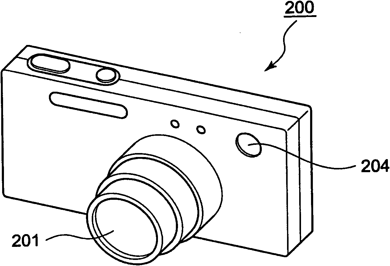
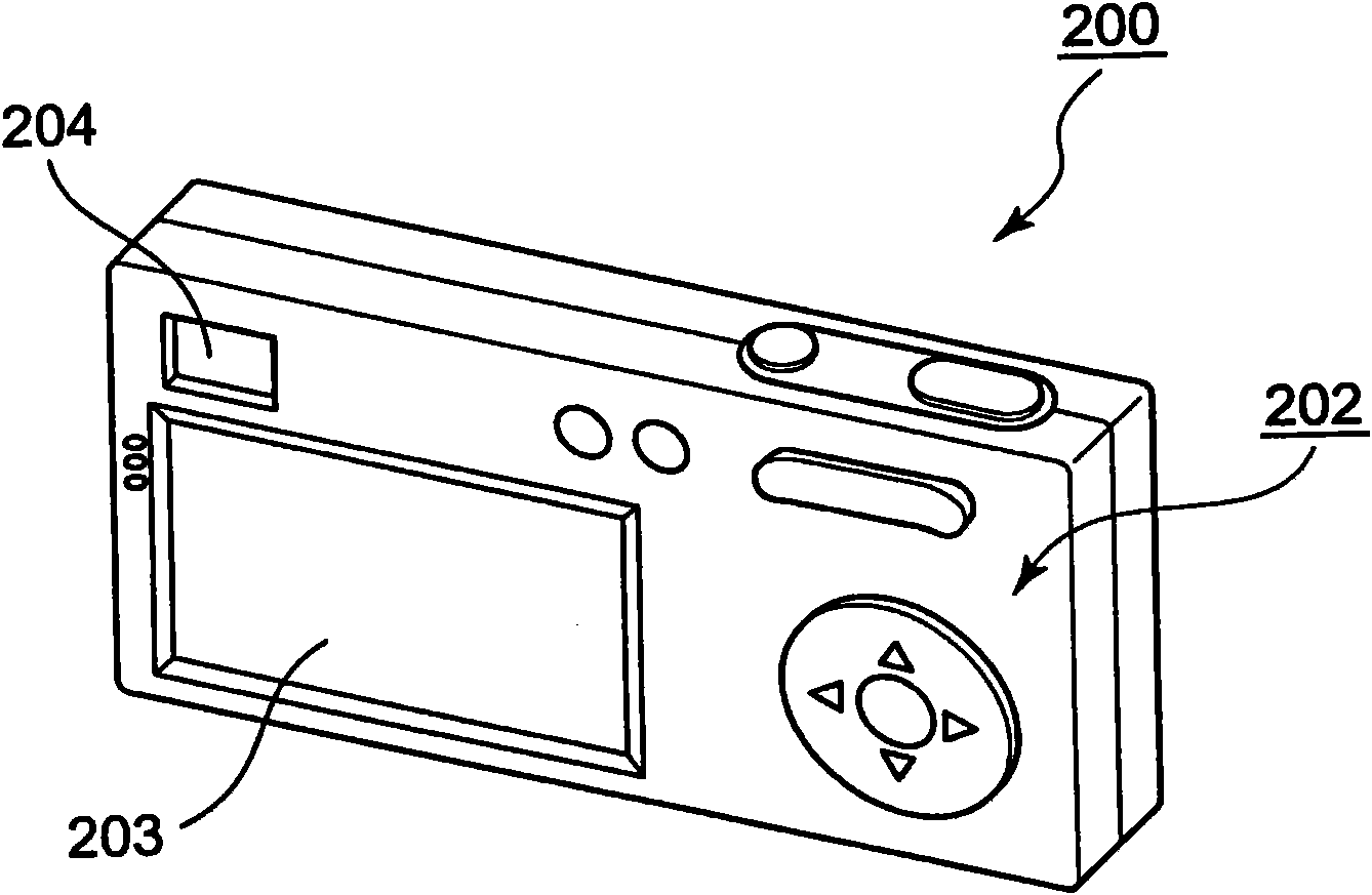
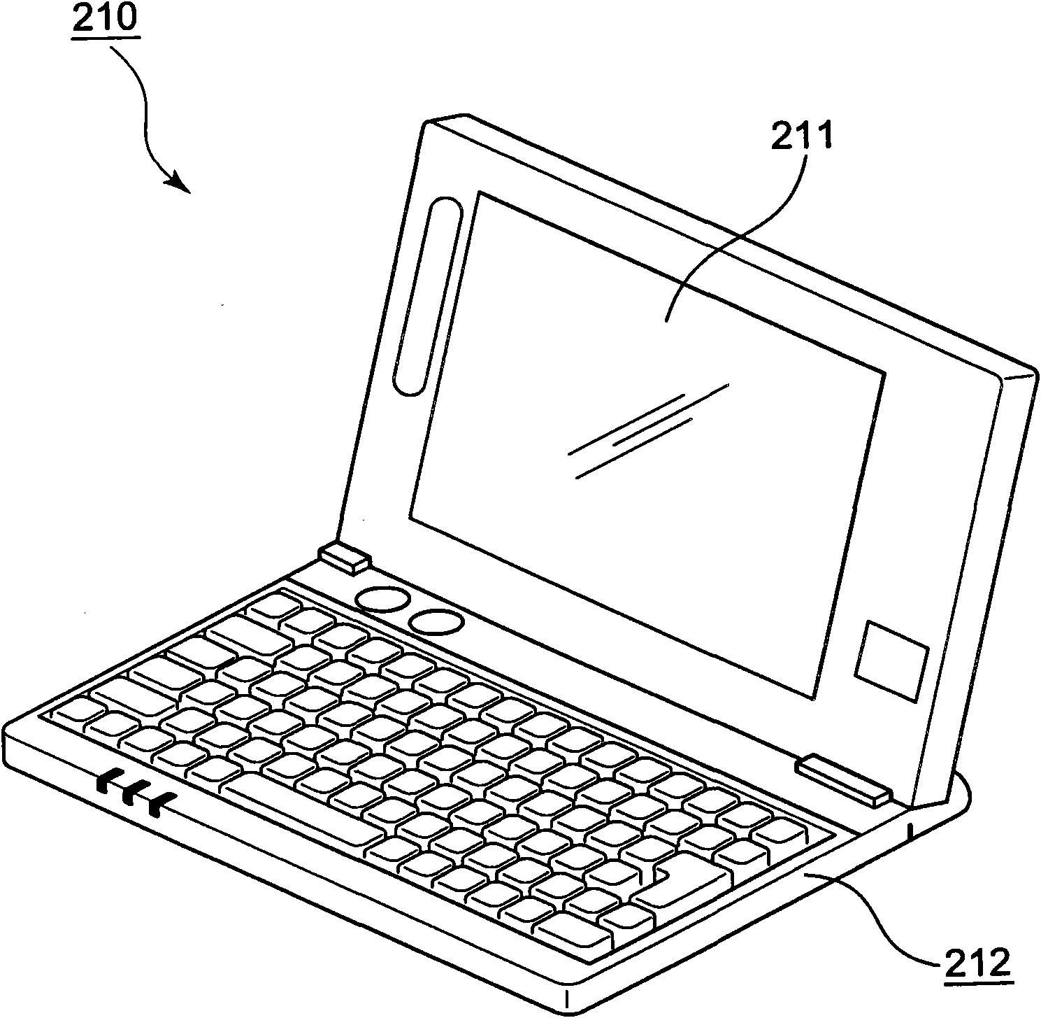
[0045] The display device 1 is assembled in the digital camera shown in FIG. 1 , figure 2 computer shown and image 3 shown in electronic equipment such as mobile phones.

[0046] like Figure 1A and Figure 1B As shown, the digital camera 200 includes a lens unit 201 , an operation unit 202 , a display unit 203 , and a viewfinder (finder) 204 . The display unit 203 is the display device 1 .

[0047] figure 2 The illustrated computer 210 includes a display unit 211 and an operation unit 212 , and the display unit 211 adopts the display device 1 .

[0048] image 3 The illustrated mobile phone 220 includes a display unit 221 , an operation unit 222 , a receiver 223 , and a microphone 224 . The display unit 221 is the display device 1 .

[0049] like Figure 4 As shown, such a display device 1 includes a TFT panel 11 , a display signal generating circuit 12 , a system controller 13 , a selection driver 14 , a power driver 15 and a data driver 16 .

[0050] The TFT panel...


PUM


Abstract

The invention provides a transistor with a reduced characteristic deviation. An electric field shielding electrode (54) is disposed between a BL insulating film (53) of a transistor and a BL insulating film (55), and a barrier film (58) is composed of the three layers. The electric field shielding electrode (54) shields the electric field of a drain electrode (T1d), a source electrode (T1s) and a n+-Si film (56). Therefore, in various driven transistors, even if the alignment dislocation of the drain electrode (T1d), the source electrode (T1s) and the n+-Si film (56) is deviated and the overlapping part with an i-Si film (52) is enlarged, the electric field of the part is shielded by the electric field shielding electrode (54), and the characteristic deviation is reduced.

Description

technical field [0001] The present invention relates to transistors, display devices, electronic equipment and methods for manufacturing transistors. Background technique [0002] In recent years, as a next-generation display device following the liquid crystal display device (LCD), a display panel equipped with a light-emitting element type in which self-emitting elements such as organic electroluminescence elements (hereinafter referred to simply as "organic EL elements") are two-dimensionally arranged Research and development of display devices (see Patent Document 1, Japanese Laid-Open Patent Publication, Japanese Patent Application Laid-Open No. 08-330600). [0003] An organic EL element includes an anode electrode, a cathode electrode, and an organic EL layer (light-emitting functional layer) having, for example, a light-emitting layer, a hole injection layer, and the like formed between the pair of electrodes. An organic EL element emits light using energy generated ...

Claims


Application Information

Patent Timeline
Patent Type & Authority Applications(China)
IPC IPC(8): H01L29/78H01L27/32H01L21/336H01L21/77H01L51/50H01L51/56
CPCH01L29/66765H01L27/1214H01L29/78648G02F1/1368G02F2001/136218H01L27/3262H01L27/12H01L27/124G02F1/136218H10K59/1213H01L29/78606H10K59/126
Inventor 宫川达也
Owner SOLAS OLED LTD
Why Eureka
Try Eureka