Static random-access memory

A static random access and memory technology, applied in static memory, digital memory information, information storage and other directions, can solve the problems of unfavorable capacity expansion and layout, too many transistors, low read and write rate, etc. Simple wiring, circuit and space saving effect

Inactive Publication Date: 2011-07-06
SHANGHAI HUAHONG GRACE SEMICON MFG CORP
View PDF3 Cites 7 Cited by
  • Summary
  • Abstract
  • Description
  • Claims
  • Application Information

AI Technical Summary

Problems solved by technology

[0010] In order to overcome the shortcomings of the SRAM in the prior art that the reading and writing rate is low due to only serial operation and that more transistors are used for the low reading and writing rate, which is not conducive to capacity expansion and layout and wiring, the main purpose of the present invention is The purpose is to provide a static random access memory, which adopts four transistors to realize a dual-port static random access memory, which achieves the purpose of increasing the read and write speed, and the circuit is simple, which is beneficial to capacity expansion and layout and wiring

Method used


Image

  • Static random-access memory
  • Static random-access memory
  • Static random-access memory

Examples


Embodiment Construction

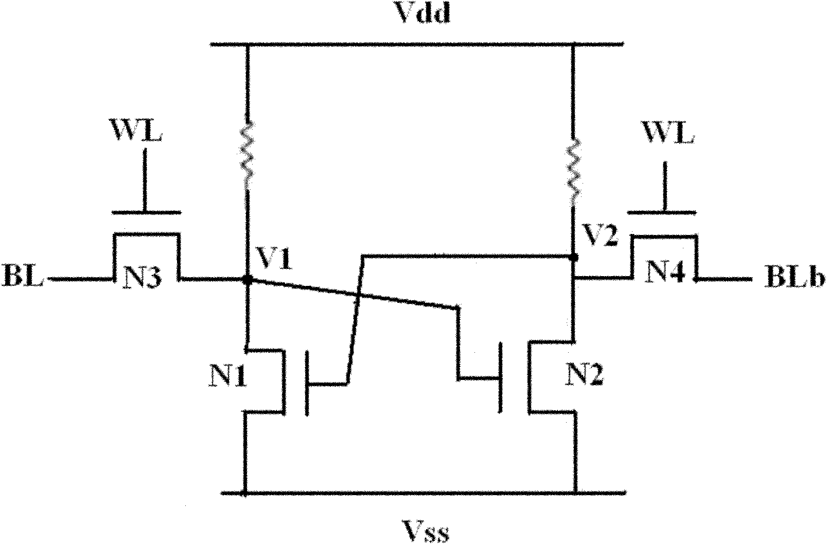
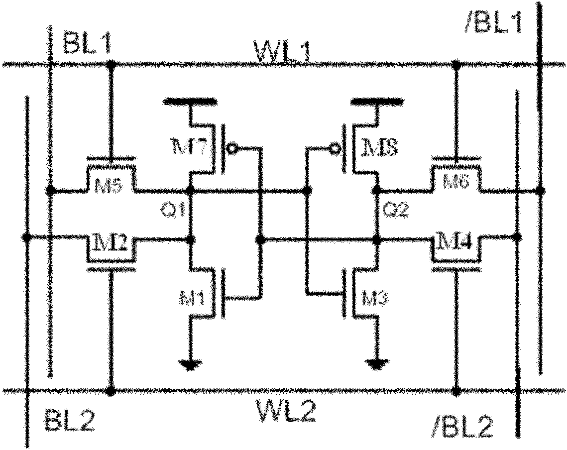
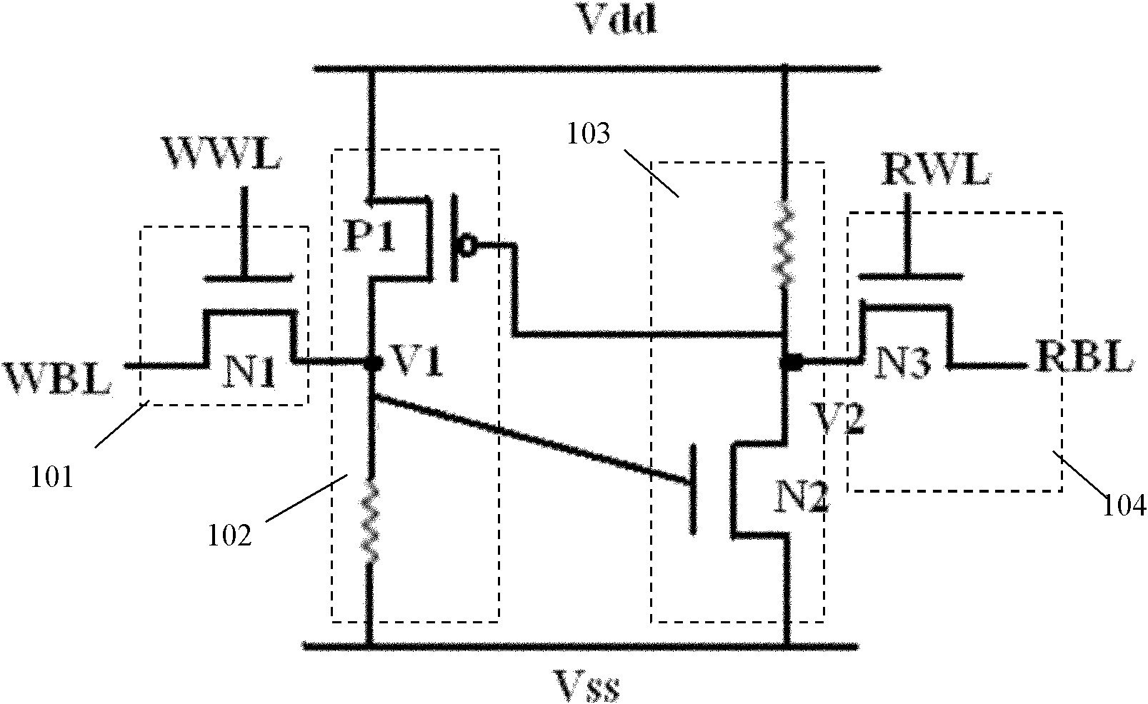
[0024] image 3 A circuit structure diagram of the best embodiment of the presence of a tuner tube static random access to the present invention.like image 3 It shows that a static random access memory of the tuner tube of the present invention includes writing control circuit modules 101, the first reverse circuit 102, the second reverse circuit 103, and the reading buffer circuit 104.Write the control circuit module 101, respectively to one write line WBL and one -word WWL, and connect with the first reverse circuit 102 to form the first storage node V1;Control circuit module 101 and one -tonal voltage source (such as grounding or VSS), which is connected with the writing control circuit module 101 to form the first storage node V1. At the same time103 and read out the buffer circuit 104 commonly connected to form a second storage node V2; the second reverse circuit 103 is connected between the first voltage source (VDD) and the complementary voltage source (such as grounding or...


PUM


Abstract

The invention discloses a static random-access memory, which comprises a writing control circuit module, a first revert circuit, a second reverse circuit and a reading-out buffer circuit, wherein the writing control circuit module is used for controlling the static random access memory to write in information; the first reverse circuit comprises a PMOS (p-channel metal oxide semiconductor) transistor and a first resistor, is coupled to the writing control circuit module to form a first storage node; the second reverse circuit comprises a second NMOS (n-channel metal oxide semiconductor) transistor and a second resistor and is connected between a voltage source and a complementary voltage source; and the reading-out buffer circuit is coupled to a word-reading line and a bit-reading line and is commonly coupled to the first reverse circuit and the second reverse circuit to form a second storage node. According to the invention, the dual-port SRAM (static random access memory) is realized by using four transistors and two resistors, so that the improvement on the reading and writing speed is facilitated, and the benefits of simple circuit, less occupied space and convenience in capacity extension and layout wiring are realized.

Description

Technical field [0001] The present invention is about a semiconductor memory device, especially about a static random access memory that uses tuitan tubes to realize dual -mouth. Background technique [0002] Static random access memory (SRAM) is often used in temporary storage data in computer systems.As long as the power supply is continuously provided, SRAM can maintain its storage status without any data update operation.The SRAM device includes a array composed of "unit", and each unit can store a "bit" data.The typical SRAM unit may include two cross -phase -connected anti -phase device and the two access transistors from the two complementary lines.The two access transistors are controlled by the word line to select or write operations.When reading the operation, the transistor is turned on to allow the charge of the storage node of the anti -phase device retained in the cross -boring pupae.When writing operation, the voltage of the transistor to the transistor and line or...

Claims


Application Information

Patent Timeline
Patent Type & Authority Applications(China)
IPC IPC(8): G11C11/413
Inventor 胡剑
Owner SHANGHAI HUAHONG GRACE SEMICON MFG CORP
Why Eureka
Try Eureka