Level switching circuit and level switching method for OTP (One Time Programmable) peripheral circuit

A conversion circuit and peripheral circuit technology, which is applied in the direction of logic circuit coupling/interface, logic circuit connection/interface arrangement using field effect transistors, etc., can solve the problems of conversion and isolation, and achieve the effect of solving conversion and isolation.

Inactive Publication Date: 2011-07-06
INST OF MICROELECTRONICS CHINESE ACAD OF SCI
View PDF0 Cites 14 Cited by
  • Summary
  • Abstract
  • Description
  • Claims
  • Application Information

AI Technical Summary

Problems solved by technology

[0014] In order to solve the problem of conversion and isolation between different level voltages in the OTP memory peripheral circuit, the purpose of the invention is to provide a kind of level conversion circuit for the OTP peripheral circuit

Method used


Image

  • Level switching circuit and level switching method for OTP (One Time Programmable) peripheral circuit
  • Level switching circuit and level switching method for OTP (One Time Programmable) peripheral circuit
  • Level switching circuit and level switching method for OTP (One Time Programmable) peripheral circuit

Examples


Embodiment Construction

[0035] The technical solution of the present invention will be described in detail below in conjunction with the accompanying drawings and embodiments.

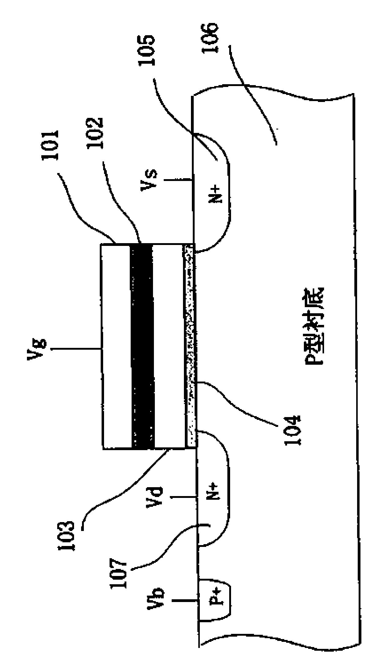
[0036] Such as Figure 4 as shown, Figure 4 The level conversion circuit for the OTP peripheral circuit proposed by the embodiment of the present invention includes a word line decoder 201, a first-level buffer BUF1, a CMOS inverter 202, a conversion latch module 203, and a second-level buffer Device BUF2, word line driving circuit 206. The input end of the first stage buffer BUF1 is connected to the word line decoder 201 , and the output end is connected to the input end of the inverter 202 . Conversion latch module 203, its input terminal is connected with the output signal IN of the first-stage buffer BUF1 and the reverse signal output by the output signal IN through the inverter 202, and its output terminal OUT is connected with the input terminal of the second-stage buffer BUF2 connected. The input end of the second...


PUM


Abstract

The invention relates to the field of voltage level switching circuit design, in particular to a level switching circuit for an OTP (One Time Programmable) peripheral circuit. The level switching circuit comprises a word line decoder (201), a first-stage buffer (BUF1), a CMOS (Complementary Metal Oxide Semiconductor) phase inverter (202), a first PMOS (P-channel Metal Oxide Semiconductor) tube (T1), a second PMOS tube (T2), a first NMOS (N-channel metal oxide semiconductor) tube (T3), a second NMOS tube (T4), a second-stage buffer (BUF2) and a word line driving circuit (206). In the level switching circuit, a level is adjusted and isolated by the PMOS tubes and the NMOS tubes, so that the level of a signal output from a low power voltage work circuit can be switched to a signal of a high power voltage and then the signal is input to a high power voltage work circuit, therefore, the problems related to the switching and the isolation of the voltage of different levels in the OTP memory peripheral circuit are solved.

Description

technical field [0001] The invention relates to the field of voltage level conversion circuit design, in particular to a level conversion circuit and a conversion method for OTP peripheral circuits. Background technique [0002] In semiconductor integrated circuit devices in recent years, non-volatile OTP memory elements that store information that will not disappear even if the power is turned off have become indispensable units. OTP memory is widely used in DRAM and SRAM large-capacity memory for backup, analog circuits for tuning and storage of key codes, and ID chips for storing history management information in the manufacturing process, etc. [0003] For example, in the memory backup application, as the cheapest non-volatile memory, a ROM using a laser fuse that stores information irreversibly by being blown by irradiation with laser light has been used. [0004] In the above-mentioned laser-fuse ROM, a special fuse blowing device and a blowing process using the devic...

Claims


Application Information

Patent Timeline
Patent Type & Authority Applications(China)
IPC IPC(8): H03K19/0185
Inventor 王琴杨潇楠刘明王永
Owner INST OF MICROELECTRONICS CHINESE ACAD OF SCI
Why Eureka
Try Eureka