Method for manufacturing inductive element

A technology of inductance components and manufacturing methods, which is applied in electrical components, inductance/transformer/magnet manufacturing, inductors, etc., can solve the problems of coil A1's large electromagnetic ratio, complicated operations, and loss.

Inactive Publication Date: 2011-07-13
TAIPEI MULTIPOWER ELECTRONICS
View PDF0 Cites 7 Cited by
  • Summary
  • Abstract
  • Description
  • Claims
  • Application Information

AI Technical Summary

Problems solved by technology

On the one hand, wire-wound inductors can use the thickness of the coil to control the current resistance, and on the other hand, the number of coils can be controlled to adjust the inductance value. The product design is more flexible, but its disadvantage is that it is larger
[0005] The current manufacturing method of making inductive components using iron-silicon alloy is to use flake or block-shaped iron-silicon alloy materials to form inductive components by assembling, please refer to Figure 10 , is a side view sectional view of an existing inductance element, and it can be clearly seen from the figure that the inductance element A includes a coil A1, and a sheet-like or block-like iron-silicon alloy material A2 is assembled outside the coil A1, In addition, the inner and outer surfaces of the iron-silicon alloy material A2 a

Method used


Image

  • Method for manufacturing inductive element
  • Method for manufacturing inductive element
  • Method for manufacturing inductive element

Examples


Embodiment Construction

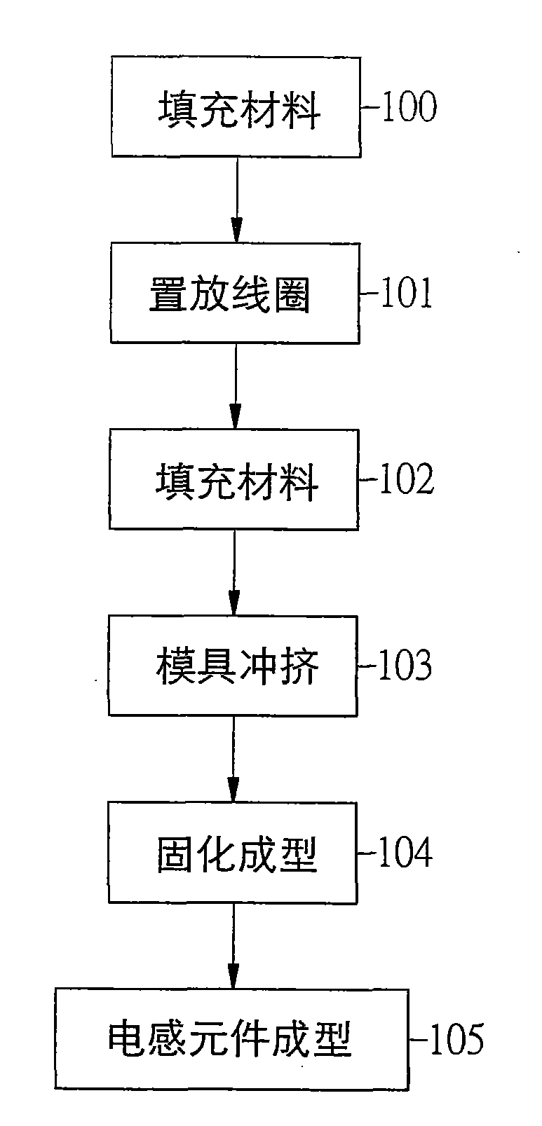
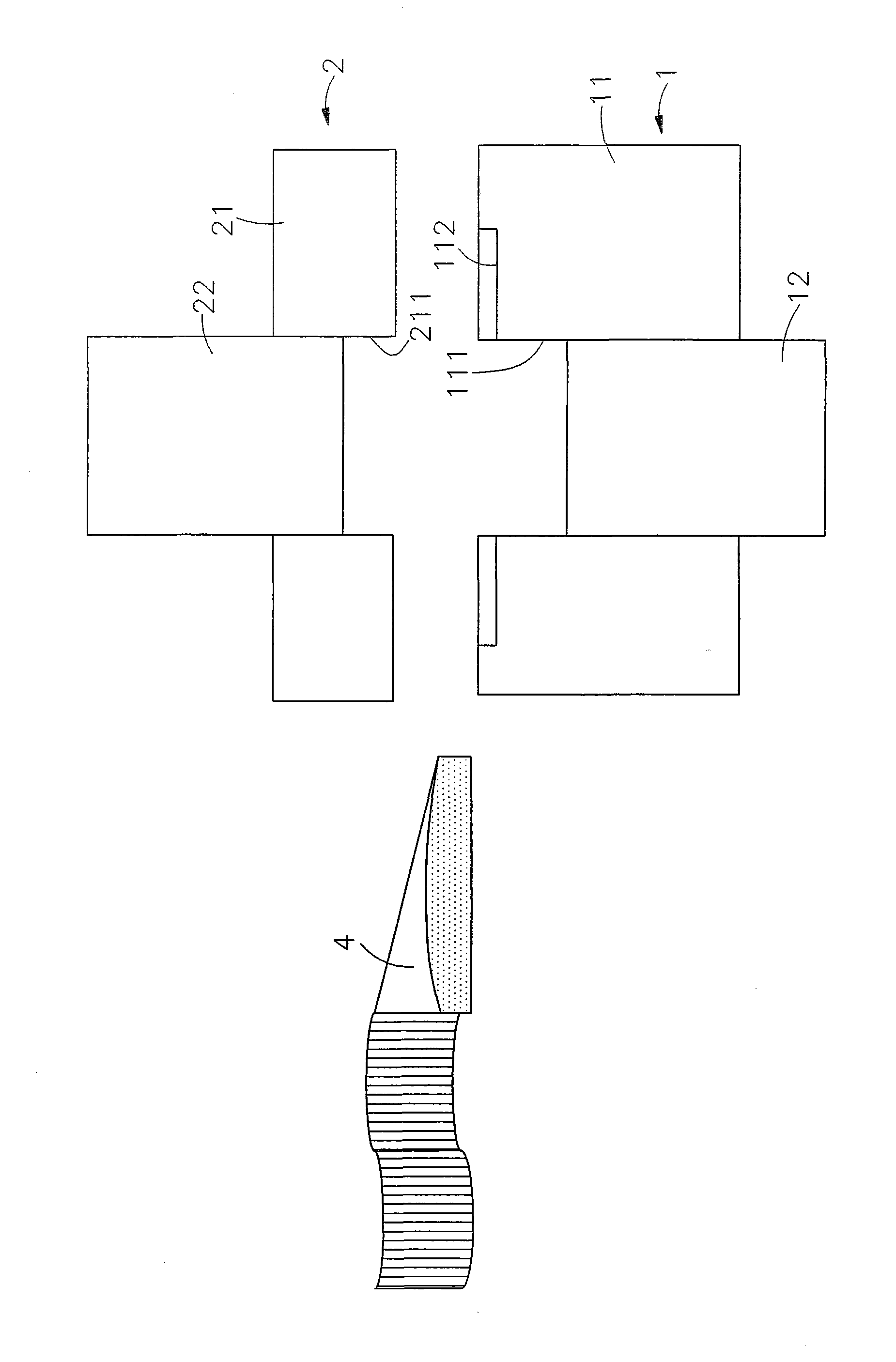
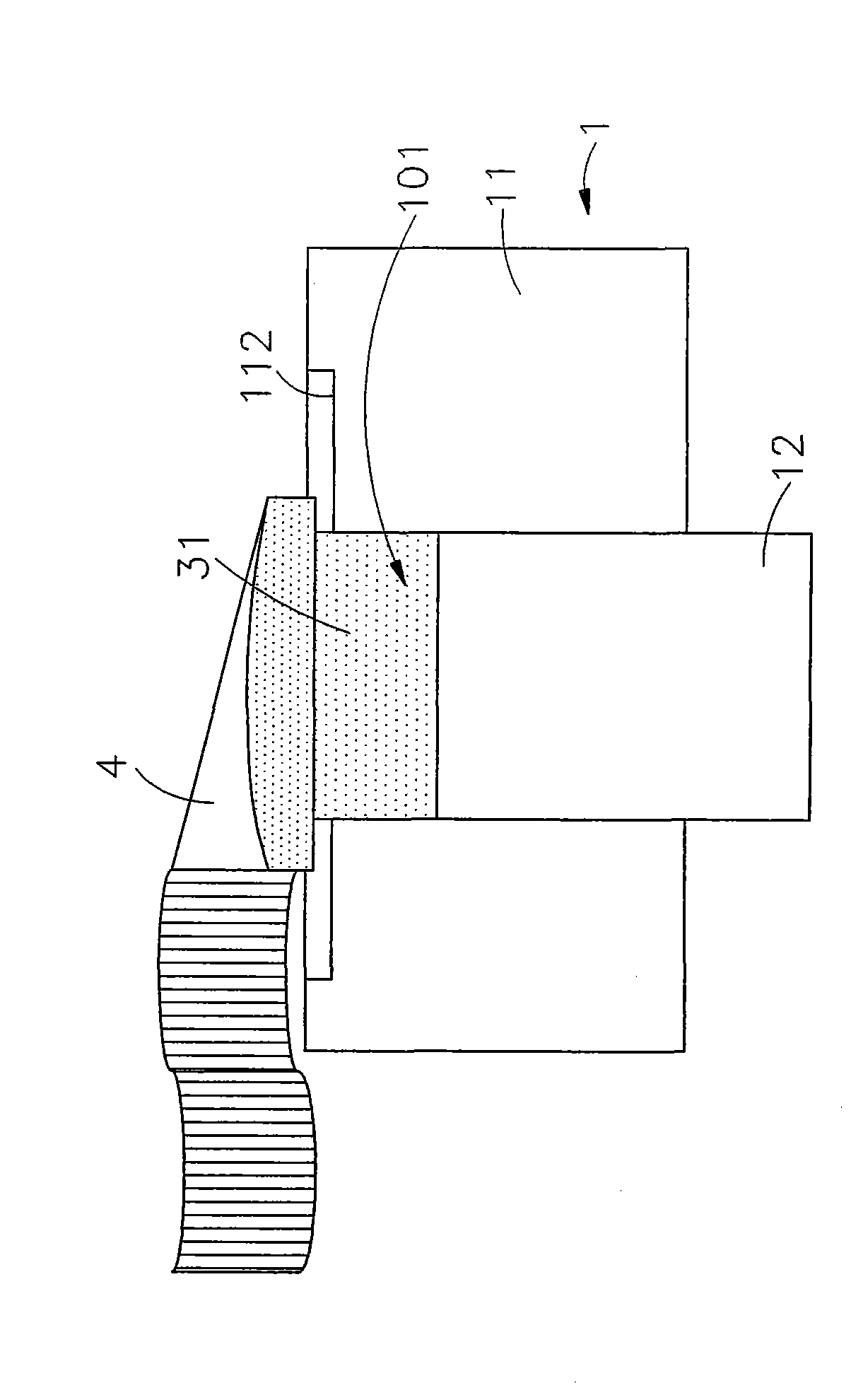
[0037] In order to achieve the above-mentioned purpose and effect, the technical means and the structure thereof adopted in the present invention are hereby illustrated in detail with respect to the preferred embodiments of the present invention. Its features and functions are as follows, so as to fully understand.

[0038] Please also refer to Figure 1 to Figure 7 , is the manufacturing flow chart of the inductance element of the present invention, the side view of the opening and closing of the lower mold core and the upper mold core, the side view of filling the iron-silicon alloy material, the side view of placing the coil on the lower mold core, and the upper mold core in the filling The side view of the position, the side view of refilling the iron-silicon alloy material, and the side view of the lower mold core and the upper mold core punching the iron-silicon alloy material can be clearly seen from the figure. The inductance element, the mold includes the lower mold c...


PUM


Abstract

The invention discloses a method for manufacturing an inductive element, comprising the steps of: manufacturing the inductive element by utilizing a die, wherein the die comprises a lower die core and an upper die core; causing the lower die core and the upper die core to relatively move to a filling position and an extrusion position along an axial direction; when the lower die core is located at the filling position, filling an iron silicon alloy material into a first space formed by the lower die core; placing a coil in the iron silicon alloy material in the first space and exposing an extension part of the coil out of the iron silicon alloy material; placing the upper die core at the filling position and filling the iron silicon alloy material into a second space formed by the upper die core to cover the coil body; then moving the upper and lower die cores to the extrusion position to ensure that the iron silicon alloy material is combined with the coil; and solidifying the iron silicon alloy material to ensure that the coil body is fixed in the iron silicon alloy material, wherein high magnetic conductivity is generated by matching the iron silicon alloy material with an integrated structure, the number of turns of the coil is reduced and the cost of the metal material of the coil is low so that the inductive element with low cost, low loss and high magnetic conductivity can be integrated.

Description

technical field [0001] The invention provides a method for manufacturing an inductance element, especially using the lower mold core and the upper mold core to move relatively between the filler position and the extrusion position, so as to manufacture an integrally formed, low-cost inductance element with low loss and high magnetic permeability . Background technique [0002] The inductance element is generally of auxiliary nature, and its main function is to hinder the change of the current to maintain the stability of the electronic product. The form of its structure can be designed in different structures according to different application circuit collocations. At present, the application lines of inductors are mainly divided into two categories, one is for signal purposes, such as energy storage and suppression of instantaneous current applications; the other is for noise suppression purposes, such as electromagnetic interference (Electromagnetic Disturbance, EMI) supp...

Claims


Application Information

Patent Timeline
IPC IPC(8): H01F17/00H01F41/00
Inventor 陈明琦
Owner TAIPEI MULTIPOWER ELECTRONICS
Why Eureka
Try Eureka