Semiconductor laser array fast and slow axis beam rearrangement device and manufacturing method

A laser array and laser beam technology, applied in the application field of laser technology, can solve the problems of difficult assembly, difficult adjustment, and poor shaping effect.

Inactive Publication Date: 2011-07-20
SHANXI FEIHONG LASER TECH
View PDF5 Cites 23 Cited by
  • Summary
  • Abstract
  • Description
  • Claims
  • Application Information

AI Technical Summary

Problems solved by technology

However, this method has certain limitations. With the increase in the number of semiconductor laser array bars, the number of optical glass sheets to be used will increase exponentially, and the cumulative error of the optical glass sheets will become larger and larger, exceeding the The tolerance range of the shaping module, the shaping effect becomes worse, there are problems of difficult assembly, large cumulative error, and difficult adjustment

Method used


Image

  • Semiconductor laser array fast and slow axis beam rearrangement device and manufacturing method
  • Semiconductor laser array fast and slow axis beam rearrangement device and manufacturing method
  • Semiconductor laser array fast and slow axis beam rearrangement device and manufacturing method

Examples


Embodiment 1

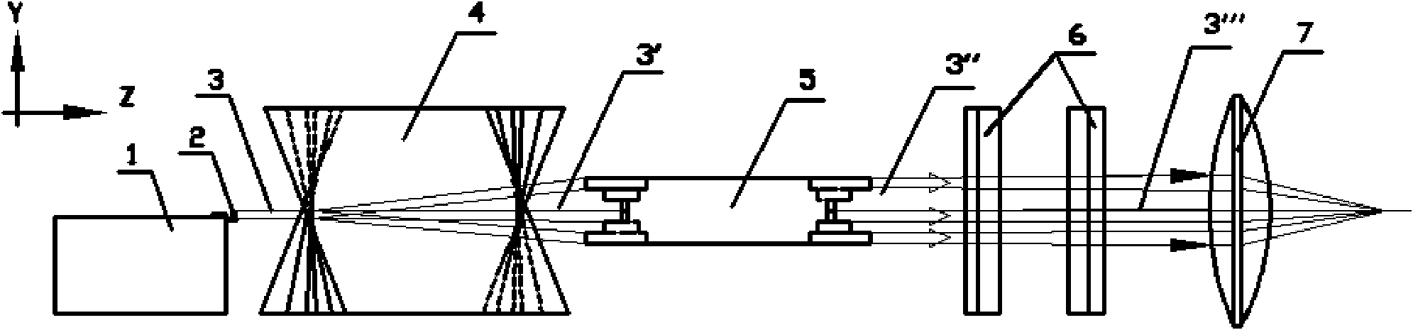
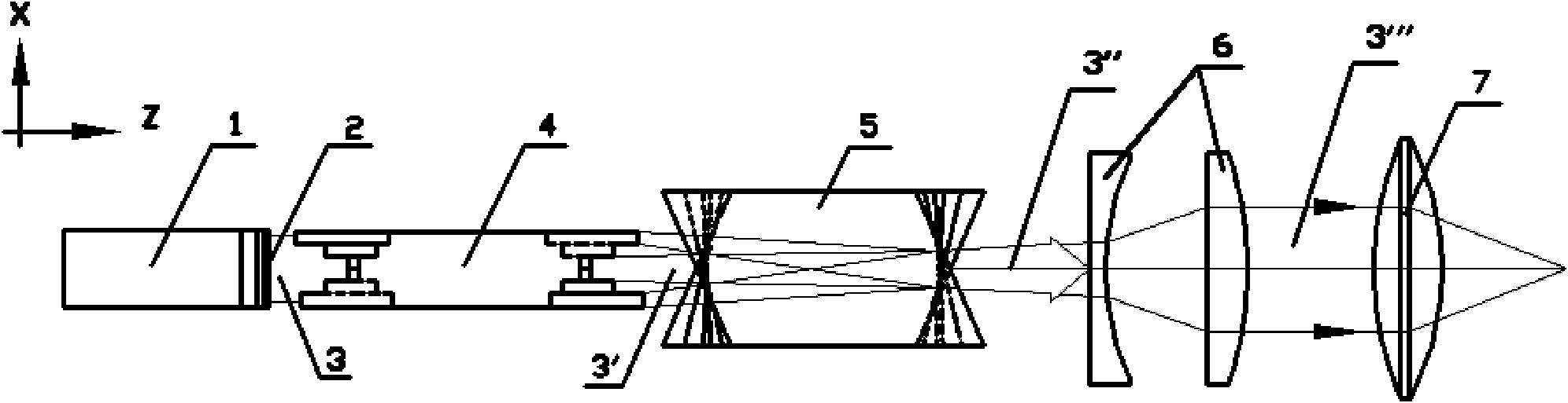
[0048] For one-dimensional semiconductor laser array, the device includes one-dimensional semiconductor laser array 1, fast and slow axis collimating microlens array 2, shaping optical element, 4, shaping optical element 5, slow axis beam expanding collimating cylindrical lens group 6 and spherical surface Focus lens 7, such as figure 1 , figure 2 Shown. In the figure, the x direction is the slow axis direction of the one-dimensional semiconductor laser array, the y direction is the fast axis direction of the one-dimensional semiconductor laser array, and the z direction is the beam transmission direction of the one-dimensional semiconductor laser array.

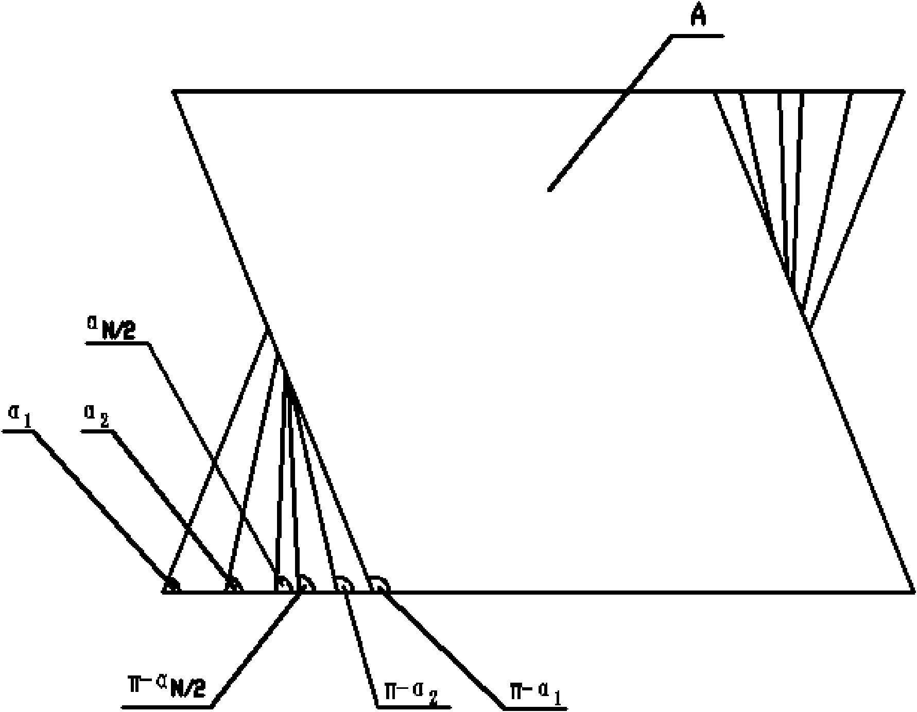
[0049] The light emitted by the one-dimensional array of semiconductor lasers is a stripe spot 3, such as Figure 7 Shown in. Through the divergence angle and spot size of the fast and slow axis of the semiconductor laser one-dimensional array, the fast axis beam quality BPP can be calculated according to the calculation form...

Embodiment 2

[0052] For the semiconductor laser two-dimensional close-packed array, the device includes a semiconductor laser two-dimensional close-packed array 8, a fast and slow axis collimating microlens array 2, a cylindrical lens group for compressing the size of the fast axis 9, a shaping optical element 4, Shaping optical element 5, slow axis beam expanding collimating cylindrical lens group 6 and spherical focusing lens 7, such as Picture 9 , Picture 10 Shown. In the figure, the x direction is the slow axis direction of the semiconductor laser two-dimensional close-packed array, the y direction is the fast axis direction of the semiconductor laser two-dimensional close-packed array, and the z direction is the beam transmission direction of the semiconductor laser two-dimensional close-packed array.

[0053] The light emitted by the two-dimensional close-packed array of semiconductor lasers is a strip-shaped spot 10, such as Picture 11 Shown in. Through the divergence angle and spot...

Embodiment 3

[0056] For the semiconductor laser two-dimensional non-close-packed array, the device includes a semiconductor laser two-dimensional non-close-packed array 11, a fast and slow axis collimating microlens array 2, a shaping optical element 4, and k shaping optical elements 5 closely arranged vertically ( k is the number of bars in the two-dimensional non-close-packed semiconductor laser array), the slow axis beam expanding collimating cylindrical lens group 6 and the spherical focusing lens 7, such as Picture 12 , Figure 13 Shown. In the figure, the x direction is the slow axis direction of the two-dimensional non-closed array of semiconductor lasers, the y direction is the fast axis direction of the two-dimensional non-closed array of semiconductor lasers, and the z direction is the beam transmission of the two-dimensional non-closed array of semiconductor lasers. direction.

[0057] The light emitted by the two-dimensional non-close-packed array of semiconductor lasers is k str...


PUM


Abstract

The invention discloses a semiconductor laser array fast-slow axis beam rearrangement device and a manufacturing method, and belongs to the field of laser technology application. By using the principle that the light produces different offsets after passing through parallel flat plates of the same thickness in different incident angles, an optical shaping element 4 and an optical shaping element 5 provided with a plurality of small surfaces are increased in the laser light path transmission process. The device can realize homogenization of fast and slow axis beam quality; by changing the conventional mode of waveguide transmission by means of a thin sheet, the loss of optical power is further reduced, and the shaping efficiency is improved; the device is particularly suitable for high-power semiconductor laser beam shaping; and meanwhile, the device has the advantages of more compact structure, no accumulated error, convenience in installation and adjustment and the like.

Description

Technical field [0001] The invention relates to the rearrangement and shaping of fast and slow axis beams of a semiconductor laser array, and introduces a device and a manufacturing method for rearranging the fast and slow axis beams of a semiconductor laser array, and belongs to the application field of laser technology. Background technique [0002] Semiconductor laser has the advantages of high electro-optical conversion efficiency, small size, light weight, etc., making its application more and more widespread. However, compared with other lasers, the beam quality of semiconductor lasers is relatively poor, the beam quality of the fast and slow axes is not uniform, the far-field light intensity is elliptical Gaussian distribution, and the focus is difficult, which limits its further development to a certain extent. In order to meet the application requirements, the beam of the semiconductor laser must first be rearranged and reshaped. The research of semiconductor lasers is ...

Claims


Application Information

Patent Timeline
Patent Type & Authority Applications(China)
IPC IPC(8): G02B27/09
Inventor 王智勇刘友强曹银花秦文斌
Owner SHANXI FEIHONG LASER TECH
Why Eureka
Try Eureka