
Preparation method of trench PMOS (positive-channel metal oxide semiconductor) enabling side wall of trench to be (110) surface

A trench sidewall and sidewall surface technology, which is applied in semiconductor/solid-state device manufacturing, electrical components, circuits, etc., can solve problems such as high interface state density, high threshold voltage, and unsatisfactory conditions, and reduce interface state and device size. The effect of reduction and cost reduction

Inactive Publication Date: 2011-07-20
SHANGHAI HUA HONG NEC ELECTRONICS
View PDF2 Cites 2 Cited by
  • Summary
  • Abstract
  • Description
  • Claims
  • Application Information

AI Technical Summary

Problems solved by technology

Because the interface state density between the gate oxide and the sidewall of the trench PMOS device with the sidewall of the (110) plane is much higher than that of the sidewall of the (100) plane, the threshold voltage is higher, which cannot meet the needs of practical applications.

Method used


Image

  • Preparation method of trench PMOS (positive-channel metal oxide semiconductor) enabling side wall of trench to be (110) surface
  • Preparation method of trench PMOS (positive-channel metal oxide semiconductor) enabling side wall of trench to be (110) surface
  • Preparation method of trench PMOS (positive-channel metal oxide semiconductor) enabling side wall of trench to be (110) surface

Examples


Embodiment Construction

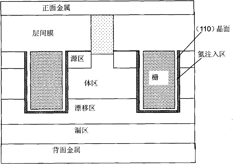
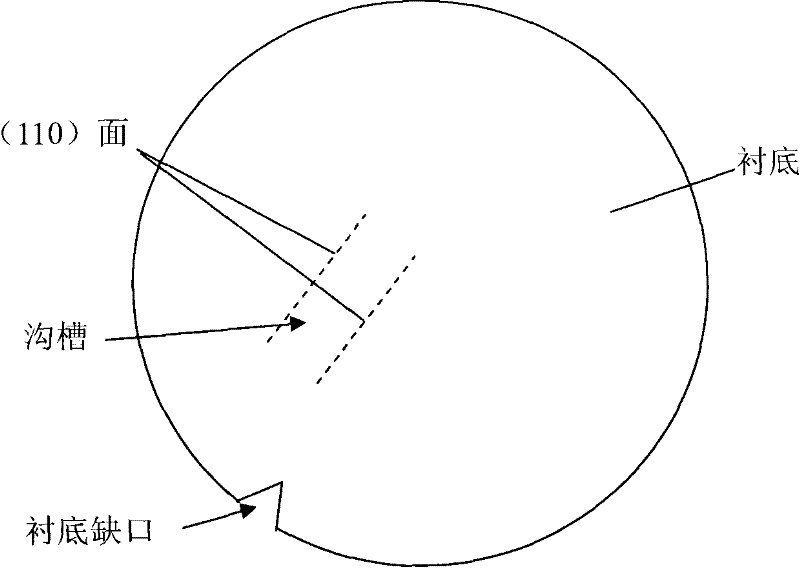
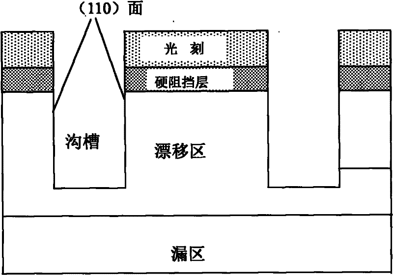
[0012] The trench sidewall of the present invention is the preparation method of the trench PMOS of (110) plane, the substrate plane used in this MOS device is (100) crystal plane, and the sidewall plane of trench is designed as (110) plane, when passing light When the etching process defines the groove pattern on the substrate, the sidewall surface of the groove after etching is made into a (110) crystal plane; after the groove is formed by etching, nitrogen ions are implanted on the inner wall of the groove; The gate oxide is grown on the inner wall of the trench. The implanted nitrogen ions greatly reduce the dangling bonds at the interface between the sidewall of the trench and the gate oxide, thereby greatly reducing the interface state, thus reducing the threshold voltage and being easy to be precisely controlled. The mobility of the PMOS majority carrier holes along the (110) crystal plane is much higher than that along the 110) crystal plane, so that the PMOS with (110...


PUM


Abstract

The invention discloses a preparation method of a trench PMOS (positive-channel metal oxide semiconductor) enabling the side wall of a trench to be the (110) surface, which comprises the following steps: enabling the side wall surface of the trench after etching to be the (110) crystal surface when defining a trench pattern on a substrate through the photoetching process; injecting nitrogen ions into the inner wall of the trench after forming the trench by etching; and then growing a gate oxide on the inner wall of the trench. By adopting the method, the threshold voltage of the PMOS device can be effectively reduced to achieve the application requirement.

Description

technical field [0001] The invention relates to a preparation method of trench PMOS, in particular to a preparation method of a trench type MOS device with vertical trenches. Background technique [0002] In existing trench MOSFET devices (see figure 1 ), the preparation of trench-type PMOS usually designs the sidewall of the trench as a (100) plane. Because the interface state density between the gate oxide and the sidewall of the trench PMOS device with the sidewall of the (110) plane is much higher than that of the sidewall of the (100) plane, the threshold voltage is higher, which cannot meet the needs of practical applications. Therefore, the industry generally only designs trench PMOS with sidewalls of (100) planes. However, the mobility of majority carrier holes along the (110) crystal plane in PMOS is much higher than that along the (110) crystal plane. Therefore, if the device threshold voltage of a trench PMOS whose trench sidewall is (110) can be lowered, its o...

Claims


Application Information

Patent Timeline
IPC IPC(8): H01L21/336H01L21/265H01L29/04
Inventor 金勤海李冰
Owner SHANGHAI HUA HONG NEC ELECTRONICS
Learn More