DC/DC converter circuit

A technology of DC converters and circuits, applied in the field of DC/DC converter circuits, can solve the problems of small overall volume and achieve the effect of reducing manufacturing costs

Inactive Publication Date: 2011-07-27
RENESAS ELECTRONICS CORP
View PDF1 Cites 6 Cited by
  • Summary
  • Abstract
  • Description
  • Claims
  • Application Information

AI Technical Summary

Problems solved by technology

Although various types exist in DC / DC converter circuits, specifically, charge pump circuits are frequently employed in portable devices because the total volume of necessary parts is small

Method used


Image

  • DC/DC converter circuit
  • DC/DC converter circuit
  • DC/DC converter circuit

Examples


no. 1 example

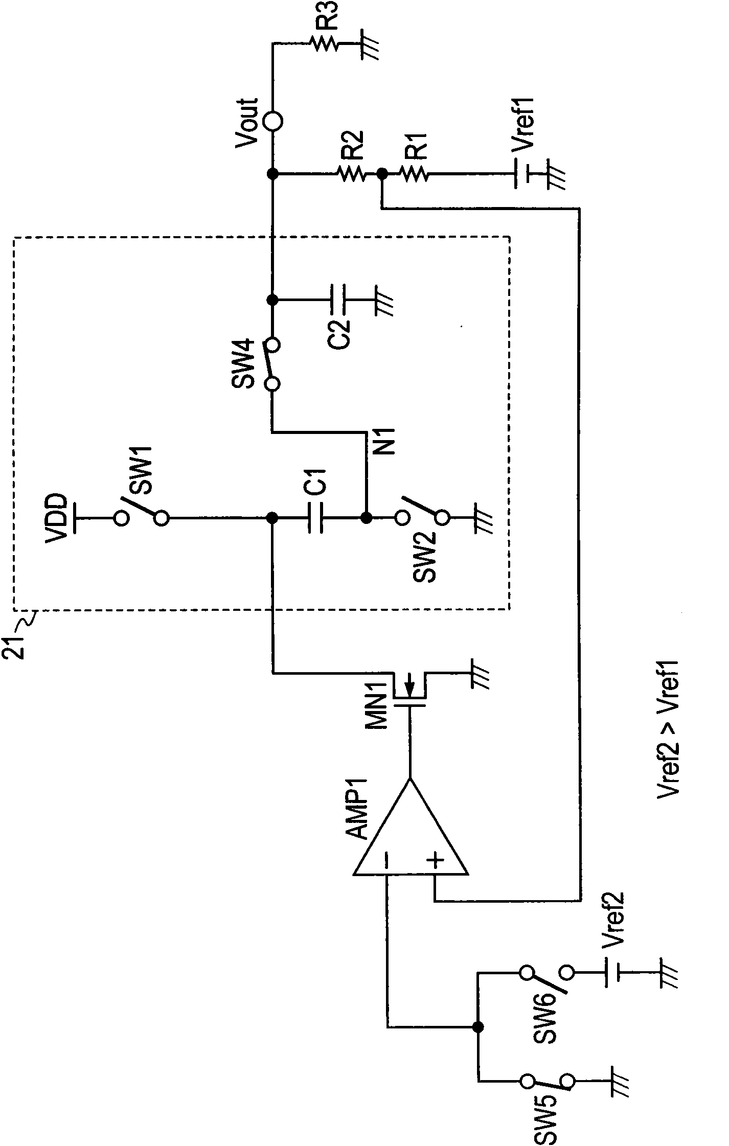
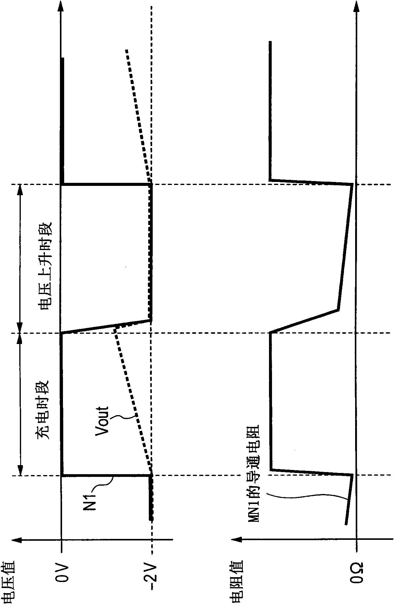
[0044] figure 1 is a circuit diagram of a DC / DC converter circuit according to a first embodiment of the present invention. The DC / DC converter circuit of the first embodiment is a voltage inversion type. exist figure 1 in, with Figure 8 The same reference numerals denote the same objects, and explanations thereof will be omitted. In addition, in figure 1 and Figure 8 Among them, the differential amplifier AMP1 and the operational amplifier 12, the voltage control resistor element MN1 and the MOSFET 14, the reference voltage Vref1 and the reference voltage Vref, and the load R3 and the load circuit 16 are the same, respectively.

[0045] exist figure 1 , by removing Figure 8 The switch SW3 in the charge pump circuit 23 constitutes the charge pump circuit 21. The junction of the switch SW4 at the end connecting the output of the charge pump circuit 21 and the capacitor C2 is connected to the output Vout and the load R3. The resistor R1 and the resistor R2 are co...

no. 2 example

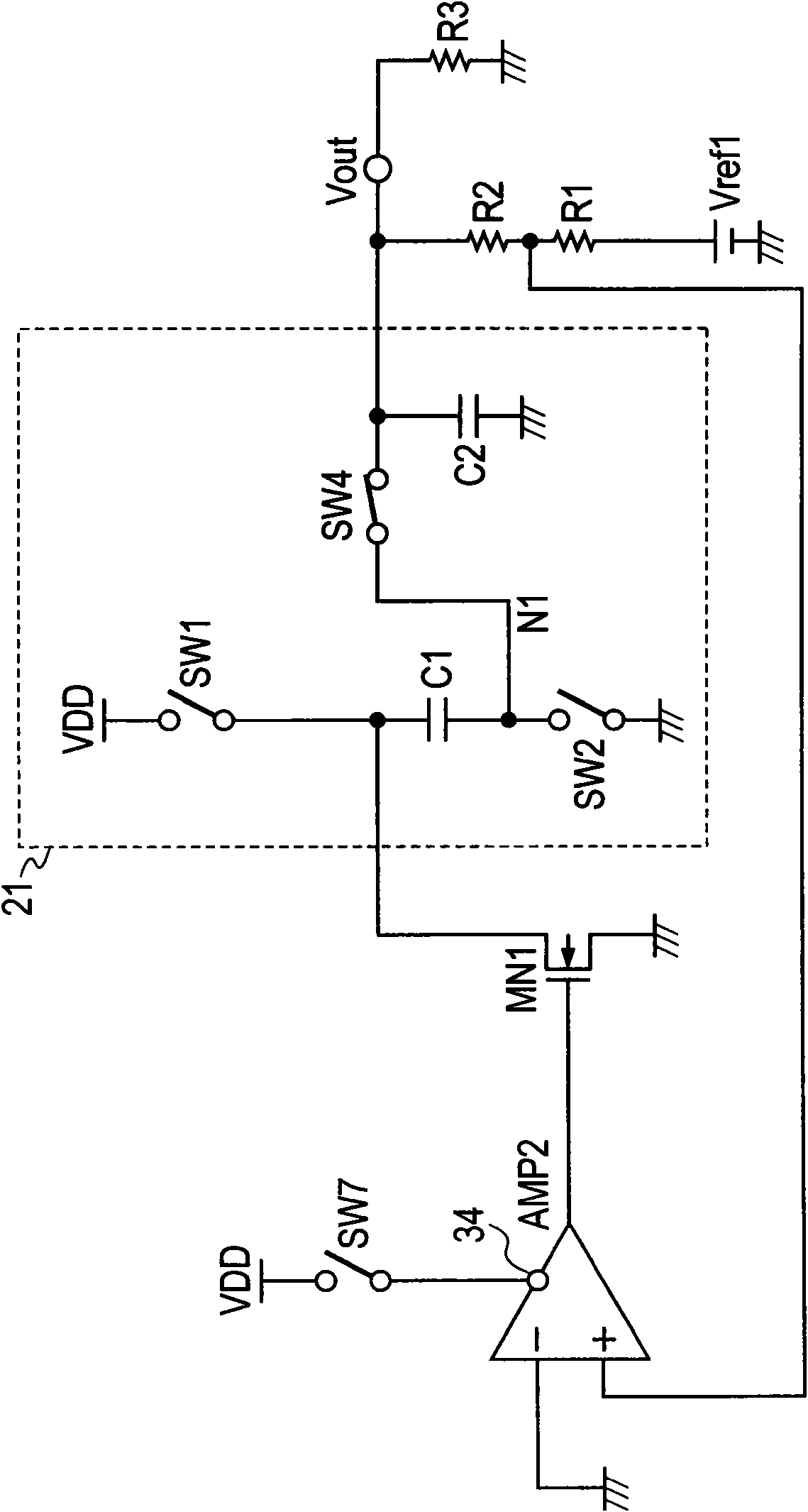
[0060] image 3 is a circuit diagram of a DC / DC converter circuit according to a second embodiment of the present invention. exist image 3 in, with figure 1 The same reference numerals denote the same objects, and explanations thereof will be omitted. The DC / DC converter circuit according to the second embodiment differs from the first embodiment as follows.

[0061] (1) The differential amplifier AMP1 is changed to a differential amplifier AMP2 having a terminal controlling the gate terminal of the output transistor (hereinafter referred to as an output control terminal 34 ).

[0062] (2) The output control terminal 34 is connected to the power supply VDD through the switch SW7.

[0063] (3) At the inverting input terminal of the differential amplifier AMP2, the inverting input terminal is connected to the ground by deleting the switches SW5 and SW6.

[0064] Figure 4 is a circuit diagram showing an example of the differential amplifier AMP2 used in the DC / DC convert...

no. 3 example

[0068] Figure 5 is a circuit diagram of a DC / DC converter circuit according to a third embodiment of the present invention. The DC / DC converter circuit according to the third embodiment is a voltage step-up type, and brings the voltage control resistor element MP1 into an off state (high resistance value) by grounding the inverting input terminal of the differential amplifier AMP1 during the charging period.

[0069] The DC / DC converter circuit according to the third embodiment is different from the first embodiment as follows.

[0070] (1) The voltage control resistor element MN1 is changed to a voltage control resistor element MP1, and its grounded end (source) is changed to be coupled to the power supply VDD.

[0071] (2) The charge pump circuit 21 of the voltage inversion type is changed to the charge pump circuit 22 of the voltage rising type. In addition, the charge pump circuit 22 is configured as follows.

[0072] The switch SW11 and the switch SW12 are respectivel...


PUM


Abstract

The present invention discloses a DC / DC converter circuit, which comprises a pump circuit of discharging electric charge charged during charging period to load during boosting period, and an amplifier and a voltage control resistor element arranged in feedback loop by being configured with the feedback loop of feeding back output voltage such that the output voltage of the charging pump circuit is made to be a predetermined value during boosting period are provided, the voltage control resistor element is controlled by the amplifier, and set to a control resistance value of enabling the charging pump circuit to control during boosting period, and the amplifier controls the voltage control resistor element such that the voltage control resistor element is brought into OFF state during charging period, and a resistance value of the voltage control resistor element is lowered to a control resistance value immediately after shifting from charging period to boosting period.

Description

[0001] Cross References to Related Applications [0002] The disclosure of Japanese Patent Application No. 2010-13095 filed on Jan. 25, 2010 including specification, drawings and abstract is hereby incorporated by reference in its entirety. technical field [0003] The present invention relates to a DC / DC converter circuit, and more particularly to a DC / DC converter circuit that stabilizes an output voltage by using a charge pump circuit. Background technique [0004] In portable devices typified by cellular phones, PDAs (Personal Digital Assistants: Portable Information Terminals), DSCs (Digital Still Cameras: Digital Still Cameras), and the like, DC / DC converter circuits are frequently used as power supply circuits that By converting the power supply voltage of about 3V, a negative power supply voltage of about -2V or a positive power supply voltage of about +5V required for LCD driving is generated. Although there are various types in DC / DC converter circuits, in partic...

Claims


Application Information

Patent Timeline
Patent Type & Authority Applications(China)
IPC IPC(8): H02M3/157
CPCH02M2003/071H02M3/07H02M3/071
Inventor 平山正彦森久司
Owner RENESAS ELECTRONICS CORP
Why Eureka
Try Eureka